Nuts & Volts
Nuts & Volts
Nuts & Volts

Create successful ePaper yourself
Turn your PDF publications into a flip-book with our unique Google optimized e-Paper software.
from the first LF444 and feed both<br />
inputs of a second LF444 through two<br />
1M resistors. We hang a capacitor off<br />
of the inverting input and — voila —<br />
the inverting input always lags the<br />
non-inverting one. As the noise<br />
voltage is taking its time trying to go<br />
up and down (due to the cap) on the<br />
inverting input, it is racing up and<br />
down on the non-inverting input.<br />
This results in the voltage on the<br />
non-inverting input randomly being<br />
higher or lower than the voltage<br />
on the inverting input as the noise<br />
voltage randomly changes. Since the<br />
op-amp is wired as a full blast<br />
comparator, its output is swinging up<br />
and down between the voltage limits<br />
of the LF444 in time to the noise<br />
fluctuations. Varying the cap and<br />
varying which input you hang the cap<br />
on will change the characteristics of<br />
BP<br />
2<br />
3<br />
LP<br />
O1<br />
O2<br />
NS<br />
1<br />
3<br />
1<br />
3<br />
1<br />
3<br />
-9V<br />
S6<br />
1<br />
SPDT<br />
R29<br />
2<br />
100K<br />
R38<br />
2<br />
100K<br />
R44<br />
2<br />
100K<br />
2<br />
2<br />
R21<br />
33K<br />
R17<br />
1<br />
150K<br />
2<br />
2<br />
1<br />
1<br />
150K<br />
2<br />
1<br />
R30<br />
R33<br />
R39<br />
2<br />
1<br />
150K<br />
2 1<br />
150K<br />
R45<br />
1K<br />
Voltage Controlled Amplifier<br />
R22<br />
1<br />
1K<br />
2<br />
R24<br />
1<br />
100K<br />
2<br />
3 +<br />
2<br />
4<br />
The Sound Lab Mini-Synth Sound Synthesizer<br />
the noise at the output of the second<br />
stage.<br />
The LFO is a simple inverting<br />
integrator with positive feedback. IC7-<br />
A ramps up when its input is held low<br />
and then ramps down when the input<br />
is brought high. IC7-B is a comparator<br />
that senses the output of IC7-A and<br />
goes high when the voltage out of<br />
IC7-A goes above its positive threshold.<br />
This high voltage is fed back to<br />
the input of IC7-A, which goes low in<br />
response until IC7-B goes low and<br />
then the cycle continues.<br />
Switch S16 and Diodes D9 and<br />
D10 control the shape of the LFO’s<br />
waveform (centered for triangle either<br />
pole gives ramp and sawtooth). In low<br />
range (S17 on), a 2 µF cap (C13) is<br />
placed in parallel with the integrator<br />
capacitor (C14) to reduce the range of<br />
frequency provided by the Frequency<br />
Voltage Controlled State Variable Filter (Band-pass and Low-pass)<br />
R34<br />
1K<br />
3 +<br />
1 7<br />
2 IC3-A<br />
LM13700 5<br />
4 11<br />
-<br />
1<br />
IC4-A<br />
LM13700<br />
-<br />
+9V<br />
1<br />
2<br />
2<br />
2<br />
1 560pF<br />
2<br />
C4<br />
R25<br />
1<br />
620K<br />
+9V<br />
R46<br />
20K<br />
R49<br />
47K<br />
1<br />
1<br />
7<br />
+9V<br />
5 8<br />
11 8<br />
BP<br />
2<br />
1<br />
-9V<br />
2<br />
R42<br />
20K<br />
8<br />
8<br />
2<br />
1<br />
2<br />
-9V<br />
R40<br />
20K<br />
R26<br />
10K<br />
2<br />
1<br />
R18<br />
1 2<br />
470K 100K<br />
R47<br />
1<br />
3<br />
R19<br />
R27<br />
2<br />
100K<br />
R48<br />
1 2<br />
20K<br />
100K<br />
1<br />
3<br />
1<br />
3<br />
pot R90.<br />
Two nine-volt batteries power the<br />
Sound Lab and the two by-pass<br />
caps absorb any large current spikes<br />
generated during operation. All of the<br />
circuits in the Sound Lab together<br />
draw less than 6 mA.<br />
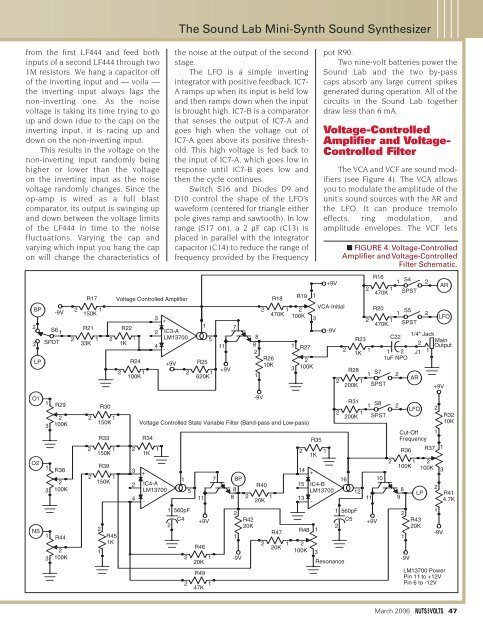
Voltage-Controlled<br />
Amplifier and Voltage-<br />
Controlled Filter<br />
The VCA and VCF are sound modifiers<br />
(see Figure 4). The VCA allows<br />
you to modulate the amplitude of the<br />
unit’s sound sources with the AR and<br />
the LFO. It can produce tremolo<br />
effects, ring modulation, and<br />
amplitude envelopes. The VCF lets<br />
+9V<br />
VCA-Initial<br />
-9V<br />
Resonance<br />
2<br />
2<br />
R28<br />
1 S7<br />
2 1<br />
200K SPST<br />
R31<br />
1 S8<br />
2 1<br />
200K SPST<br />
+9V<br />
R16<br />
1<br />
470K<br />
R20<br />
1<br />
470K<br />
1 S4<br />
2<br />
2<br />
SPST<br />
1 S5<br />
SPST<br />
2<br />
1<br />
-9V<br />
1/4" Jack<br />
2<br />
Main<br />
Output<br />
J1 1<br />
AR<br />
LFO<br />
R43<br />
20K<br />
2<br />
2<br />
+9V<br />
2<br />
1<br />
-9V<br />
AR<br />
LFO<br />
LM13700 Power<br />
Pin 11 to +12V<br />
Pin 6 to -12V<br />
R32<br />
10K<br />
Cut-Off 1<br />
R35<br />
Frequency<br />
2 1<br />
R36<br />
R37 1<br />
1K<br />
2 1 2<br />
100K<br />
14<br />
100K 3<br />
+<br />
16<br />
10<br />
15 IC4-B<br />
2<br />
LM13700 12 8<br />
LP R41<br />
13 11 9<br />
-<br />
4.7K<br />
1<br />
2<br />
■ FIGURE 4. Voltage-Controlled<br />
Amplifier and Voltage-Controlled<br />
Filter Schematic.<br />
2<br />
560pF<br />
C5<br />
R23<br />
1K<br />
1<br />
C22<br />
1 2<br />
1uF NPO<br />
March 2006 47