biographical summary of robert j. nemanich - Department of Physics ...
biographical summary of robert j. nemanich - Department of Physics ...
biographical summary of robert j. nemanich - Department of Physics ...

Create successful ePaper yourself
Turn your PDF publications into a flip-book with our unique Google optimized e-Paper software.
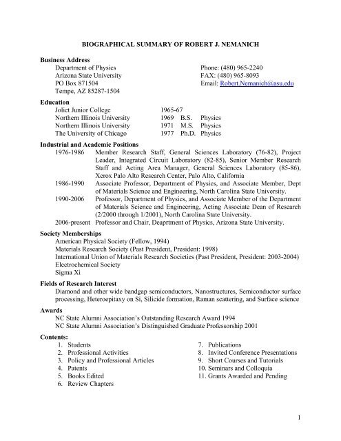
BIOGRAPHICAL SUMMARY OF ROBERT J. NEMANICH<br />
Business Address<br />
<strong>Department</strong> <strong>of</strong> <strong>Physics</strong> Phone: (480) 965-2240<br />
Arizona State University FAX: (480) 965-8093<br />
PO Box 871504 Email: Robert.Nemanich@asu.edu<br />
Tempe, AZ 85287-1504<br />
Education<br />
Joliet Junior College 1965-67<br />
Northern Illinois University 1969 B.S. <strong>Physics</strong><br />
Northern Illinois University 1971 M.S. <strong>Physics</strong><br />
The University <strong>of</strong> Chicago<br />
Industrial and Academic Positions<br />
1977 Ph.D. <strong>Physics</strong><br />
1976-1986 Member Research Staff, General Sciences Laboratory (76-82), Project<br />
Leader, Integrated Circuit Laboratory (82-85), Senior Member Research<br />
Staff and Acting Area Manager, General Sciences Laboratory (85-86),<br />
Xerox Palo Alto Research Center, Palo Alto, California<br />
1986-1990 Associate Pr<strong>of</strong>essor, <strong>Department</strong> <strong>of</strong> <strong>Physics</strong>, and Associate Member, Dept<br />
<strong>of</strong> Materials Science and Engineering, North Carolina State University.<br />
1990-2006 Pr<strong>of</strong>essor, <strong>Department</strong> <strong>of</strong> <strong>Physics</strong>, and Associate Member <strong>of</strong> the <strong>Department</strong><br />
<strong>of</strong> Materials Science and Engineering, Acting Associate Dean <strong>of</strong> Research<br />
(2/2000 through 1/2001), North Carolina State University.<br />
2006-present Pr<strong>of</strong>essor and Chair, Deaprtment <strong>of</strong> <strong>Physics</strong>, Arizona State University.<br />
Society Memberships<br />
American Physical Society (Fellow, 1994)<br />
Materials Research Society (Past President, President: 1998)<br />
International Union <strong>of</strong> Materials Research Societies (Past President, President: 2003-2004)<br />
Electrochemical Society<br />
Sigma Xi<br />
Fields <strong>of</strong> Research Interest<br />
Diamond and other wide bandgap semiconductors, Nanostructures, Semiconductor surface<br />
processing, Heteroepitaxy on Si, Silicide formation, Raman scattering, and Surface science<br />
Awards<br />
NC State Alumni Association’s Outstanding Research Award 1994<br />
NC State Alumni Association’s Distinguished Graduate Pr<strong>of</strong>essorship 2001<br />
Contents:<br />
1. Students<br />
2. Pr<strong>of</strong>essional Activities<br />
3. Policy and Pr<strong>of</strong>essional Articles<br />
4. Patents<br />
5. Books Edited<br />
6. Review Chapters<br />
7. Publications<br />
8. Invited Conference Presentations<br />
9. Short Courses and Tutorials<br />
10. Seminars and Colloquia<br />
11. Grants Awarded and Pending<br />
1
1. Students<br />
Graduate Students<br />
Charles Doland, PhD., Univ <strong>of</strong> Houston (Adjunct Faculty), Spring 88, “Molybdenum<br />
Silicide Formation on Single Crystal, Polycrystallilne and Amorphous Silicon:<br />
Growth, Structure and Electrical Properties.”<br />
Robert E. Shroder, MS, Fall 88 (Current Address; TWR, Redondo Beach, CA (as <strong>of</strong><br />
12/96), “Diamond and Diamond-Like Thin Films: A Raman Scattering Analysis<br />
<strong>of</strong> Carbon Bonding.”<br />
Robert Fiordalice, MS, Fall 88 (Current Address; Motorolla APRDL, Austin, TX),<br />
“Raman Characterization <strong>of</strong> the Ti/Si Thin Film System.”<br />
Yvonne LeGrice, MS, Fall 89 (Current address; Applied Materials), “Raman and Infrared<br />
Characterization <strong>of</strong> Diamond Thin Films.”<br />
Hyeongtag Jeon, (PhD, Materials Science and Engineering), Fall 90 (Current address<br />
Honyang University), “Initial Reactions, Surface and Interface Morphologies,<br />
Phases Transition, and Epitaxial Growth <strong>of</strong> TiSi2 Formed by Thin Film Reaction<br />
in Ultrahigh Vacuum.”<br />
John LaBrasca, MS, Spring 91 (Current address: Intel, Portland, OR), “Scanning<br />
Tunneling Microscopy and Spectroscopy <strong>of</strong> Doped Silicon and Titanium Silicide<br />
Thin Films.”<br />
Cathy Sukow, MS, Fall 92 (Current address; Brandeis University - Biophysics program),<br />
“Morphology and Mechanisms <strong>of</strong> ZrSi2 and TiSi2 on Silicon.”<br />
Jaewon Cho, PhD, Fall 92 (Current address; Seoul, Korea), “Surface Structure and<br />
Surface Electronic States Related to Plasma Cleaning <strong>of</strong> Si and Ge.”<br />
Kevin Turner, PhD, Fall 92 (Current address; Naval Research Laboratories), “A Study <strong>of</strong><br />
the Nucleation and Growth <strong>of</strong> Diamond on Silicon by Scanning Tunneling<br />
Microscopy and Spectroscopy.”<br />
Jaap van der Weide, (PhD) Fall 93, (Current Address: Waltham, MA) “Properties <strong>of</strong><br />
Diamond Surfaces and Metal-Diamond Interfaces: Schottky Barrier Heights and<br />
Negative Electron Affinity Effects.”<br />
Thomas Schneider, (PhD) Spring 94, (Current Address: Texas Instruments, 13536 N.<br />
Central Expressway, MS 944, Dallas, TX 75243) “Hydrogen Plasma Interactions<br />
with Silicon Surfaces.”<br />
Shawn Wagoner, (MS) Summer 94, (Current Address: Micron Technology, Boise, ID).<br />
“Nucleation and Growth <strong>of</strong> Homoepitaxial Diamond Films.”<br />
Julian Selvaraj, (MS) Summer 94, (Current Address: Intel Corp, Oregon) “Photophoretic<br />
Deflection <strong>of</strong> Particles in Subatmospheric Pressure Chambers.”<br />
Terri McCormick, (MS chair) Summer 1994 “The Characterization <strong>of</strong> Strain, Impurity<br />
Content and Crush Strength <strong>of</strong> Single Crystal Diamonds.” (Current Address:<br />
Harris Semiconductor, Melbourne FL. (Senior Reliability Engineer).<br />
David Aldrich, (PhD co-chair) Spring 1995 "Characterization <strong>of</strong> the Solid Phase<br />
Reaction <strong>of</strong> Titanium with Silicon Germanium Alloys: Interface Reactions, Phase<br />
Formation, and Stability." Current Address: Texas Instrument, Semiconductor<br />
Process & Design Center, Dallas, TX.<br />
2
Leah Bergman, (PhD chair) Spring 1995 ). “Photoluminescence and Raman Analysis <strong>of</strong><br />
Impurities and Defects in Diamond Films.” Current Address: University <strong>of</strong> Idaho,<br />
Moscow, Idaho.<br />
Eric Watko, (MS chair) Spring 1995 “In situ Characterization <strong>of</strong> Oxide Thin Film<br />
Growth.”(Current Address: Raleigh, NC)<br />
Mike Powers, (MS chair) Summer 1995 )."Photoemission from BN and Secondary<br />
Electron Emission from Negative Electron Affinity Surfaces." Current Address:<br />
MKE Quantum Components, Shrewsbury, MA.<br />
Yuan Dao, (PhD co-chair) Fall 1995 “Growth and Characterization <strong>of</strong> (Ti1-xZrxSi2) Thin<br />
Films on Silicon.” Current Address: Texas Instrument, Dallas, TX.<br />
Jay Montgomery, (PhD chair) December 14, 1995. “Materials and Device Analysis <strong>of</strong><br />
Hydrogen Plasma Prepared Silicon Surfaces,” Current Address: Intel, Santa<br />
Clara, CA.<br />
Ja-Hum Ku, (PhD chair) December 19, 1995 “Properties <strong>of</strong> SixGe1-x Alloy Surfaces and<br />
Co/SixGe1-x Interfaces.” Current Address: Samsung Electronics, Korea.<br />
Michael Netzer, (MS chair), November 1996 “Emission Studies <strong>of</strong> Diamond and Cubic<br />
Boron Nitride Crystallites Bonded to Metalllic Substrates.” Current Address:<br />
Harris Semiconductor, P. O. Box 883, MS 59-055, Melbourne, FL 32902-0883.<br />
Sean King, (PhD co-chair) March 25, 1997, “Surface and Interface Characterization <strong>of</strong><br />
SiC and III-V Nitrides.” Current address: Intel, RA1-234, 5200 NE Elam Young<br />
Pkwy, Hillsboro, OR 97124-6497.<br />
John Barnak, (PhD chair) June 24, 1997 “Processing <strong>of</strong> Si(100) Surfaces by a Remote RF<br />
H2 and H2/SiH4-Plasma to Remove Surface Contaminants”. Current Address:<br />
Intel, Oregon<br />
Peter Baumann, (PhD chair) July, 1997 “Electron Affinity and Electron Emission from<br />
Diamond Surfaces and Metal-Diamond Interfaces.” Current Address: Aixtron,<br />
Germany.<br />
Mark Benjamin, (PhD chair) December 1997, “Electronic Properties <strong>of</strong> SiC and AlN<br />
Surfaces and Interfaces.” Current Address: new job as <strong>of</strong> Spring 2002.<br />
Andy Stoltz (MS) January 1998, “Interface Stability <strong>of</strong> Tintanium Silicide on 6H-Silicon<br />
Carbide (0001).” Current Address: Triangle, VA.<br />
Steve English (MS chair) September 1998, Current Address: Allied Signal, Maryland,<br />
“Photoemission Electron Microscopy <strong>of</strong> Diamond Thin Films.”<br />
Hong Ying, (PhD chair) October 1998, “In-Situ Remote RF Plasma Cleaning and Surface<br />
Characterization after SiO2/Si RIE.” Current Address: LSI Logic, San Jose,CA.<br />
Ambika Somashekhar Carter (MS chair) October 1998, “The Investigation <strong>of</strong> Hydrogen<br />
Plasma Processing for Backend Cleaning.”Current Address: IMEC, Leuven,<br />
Belgium<br />
Andy Sowers, (PhD chair) January 1999, “Characterization <strong>of</strong> Field Emission Properties<br />
<strong>of</strong> Nitrogen-Doped Diamond.” Current Address: Intel, San Jose, CA.,<br />
Peter Goeller, (PhD co-chair) May 1999, “Cobalt Disilicide Contacts to Si1-xGex Alloys.”<br />
Current Address: Texas.<br />
Jim Christman, (PhD chair), August 1999, “Piezoelectric Measurments Using an Atomic<br />
Force Microscope.” Current Address: Intel, San Jose, CA,<br />
3
Richard J. Carter, (PhD chair) September 1999, “Surface Morphology and Chemical<br />
Characterization <strong>of</strong> Si Surfaces Prepared with HF/Alcohol Vapor Phase<br />
Chemistries.” Current Address: Post Doc at IMEC, Leuven, Belgium.<br />
Hoon Ham, (PhD chair) November 1999, “Scanning Tunneling Microscopy <strong>of</strong> Nanoscale<br />
Structures <strong>of</strong> Titanium Disilicide on Clean Silicon Surfaces.”Current Address:<br />
Serome Ventures, Korea.<br />
Michael O’Brien, (PhD chair) October 1999, “Photoemission <strong>of</strong> Silicon Carbide Surfaces<br />
and Interfaces.” Current Address: Northrup-Grumann, Maryland.<br />
Brandon L.Ward, (PhD chair), February 2000, “Correlation <strong>of</strong> Surface Properties with<br />
Electron Emission Characteristics for Wide Bandgap Semiconductors.” Current<br />
Address: Intel Corp., Santa Clara, CA.<br />
Kieran M. Tracy, (PhD co-chair) September 2000, “Deposition and Electrical, Chemical<br />
and Microstructural Characterization <strong>of</strong> the Interface Formed between Pt, Au and<br />
Ag Rectifying Contacts and Cleaned n-typed GaN (0001) Surfaces.” Current<br />
Address: Intel Corporation, Santa Clara, CA.<br />
Jeff Hartman, (PhD co-chair) October 2000, “Characterization <strong>of</strong> the Growth <strong>of</strong><br />
Aluminum Nitride and Gallium Nitride Thin Films on Hydrogen Etched and/or<br />
cleaned 6H-SiC(0001) Surfaces.” Current Address Northrup-Grumann, Maryland.<br />
Christian Petrich, (MS). Dec. 2000, Current Address: New Zealand, “Thermostability <strong>of</strong><br />
the 6H-SiC(0001)Si Surface Observed with Photo-Emission Electron Microscopy<br />
(PEEM).”<br />
Woochul Yang, (PhD chair), February 2001, “In Situ, Real Time Characterization and<br />
Growth <strong>of</strong> Metal Silicide Islands on Si Surfaces by Photo Electron Emission<br />
Microscopy,” Current Address: NCSU, Post doc.<br />
Jaehwan Oh (PhD chair), July 2001, “Electrical Characterization <strong>of</strong> TiSi2 Nanoscale<br />
Islands by Scanning Probe Microscopy.” Current Address: Intel, Hillsboro,<br />
Oregon.<br />
Morgan Ware (PhD chair), January 2002, “Effects <strong>of</strong> Strain Relaxation in SiGe Growth<br />
on Uniquely Oriented Si Substrates.” Current Address: Naval Research Lab,<br />
Washington, DC.<br />
Philip Hartlieb (PhD-co-chair), February 2002, “Electrical, Chemical, and Structural<br />
Characterization <strong>of</strong> the Interface Formed between Ni/Au and Pd/Au Ohmic<br />
Contacts and Cleaned p-type GaN (0001) Surfaces,” Current address: Clemson<br />
University.<br />
Franz A. M. Koeck (MS chair), 2003 “Thermionic Emission from Doped and<br />
Nanocrystalline Diamond”<br />
Ted Cook, Jr. (PhD co-chair), May 2003, “Photoemission Investigation <strong>of</strong> the Electronic<br />
Properties <strong>of</strong> Ga-Face GaN (0001)-Dielectric Interfaces”<br />
Jaeseob Lee (PhD co-chair), May 2003 “Direct Bonding <strong>of</strong> Gallium Nitride to Silicon<br />
Carbide: Physical, and Electrical Characterization” (Current address: Univ <strong>of</strong> Ill.,<br />
Post doc)<br />
Brian Coppa (PhD co-chair) June 2003, “Electrical, Chemical, and Structural<br />
Characterization <strong>of</strong> Au Schottky Contacts on Remote Plasma-Treated n-Type<br />
ZnO{0001}” (Current address: Micron Semiconductor, Idaho)<br />
4
Brian Rodriguez (PhD chair) Oct. 2003 “Nanoscale Investigation <strong>of</strong> the Piezoelectric<br />
Properties <strong>of</strong> Perovskite Ferroelectrics and III-Nitrides,” (current address: NC<br />
State, post doc.)<br />
James Burnett, (PhD co-chair) March 2, 2004 “Formation <strong>of</strong> Metal Silicide and Metal<br />
Germanosilicide Contacts to Si1-xGex Alloys,”<br />
Yunyu Wang, (PhD chair) Oct. 29, 2004, “Synthesis and Field Emission Properties <strong>of</strong><br />
Carbon Nanotube Films,” (current address: Univ <strong>of</strong> Texas, post doc)<br />
Jennifer Huening, (MS chair) Nov. 01, 2004, “Raman Scattering Analysis <strong>of</strong> Structural<br />
Transformations due to Precision Engineered Si, 6H-SiC and B-Si3N4,” (Current<br />
Address: Intel, Hillsboro, Oregon)<br />
Charles Fulton (PhD chair) Aug 2005 “Spectroscopic Study <strong>of</strong> the Interface Chemical<br />
and Electronic Properties <strong>of</strong> High-K Gate Stacks,” (Current address: Intel,<br />
Phoenix AZ)<br />
Jacob Garguilo (PhD Chair) Nov 2006, “Electronic Transition Imaging <strong>of</strong> Carbon Based<br />
Materials: The Photothreshold <strong>of</strong> Melanin and Thermionic Field Emission from<br />
Diamond”<br />
Matt Zeman (PhD)<br />
Yingjie Tang (PhD)<br />
Joshua Smith (PhD)<br />
Eugene Bryan (MS)<br />
Anderson Sunda-Meya (PhD)<br />
Xinhua (Wendy) Kong (PhD)<br />
Leigh Winfrey (PhD)<br />
James Perkins (PhD)<br />
Joe Tedesco (PhD)<br />
Jacqueline Hanson (PhD)<br />
Benjamin Gilbert (MS)<br />
Jiyoung Choung (PhD)<br />
Ed Hurt (MS)<br />
Post Docs/Visiting Scholars Mentored<br />
Leah Bergman<br />
Boyan Boyanov<br />
Y. L. Chen<br />
Anne Edwards<br />
Trevor Humphries<br />
Hyeongtag Jeon<br />
Eliane Maillard-Schaller<br />
Koichi Naniwae, Visiting Scholar<br />
Willie Platow<br />
Arilza de Oliveira Porto, Visiting Scholar<br />
Zhihai Wang<br />
Peichun Yang<br />
Woochul Yang<br />
Sanju Gupta<br />
Brian Rodriguez<br />
5
International Visiting Students (Diplom research etc.)<br />
Boike Kropman, 92, (Twente University, Holland)<br />
Michiel Slotboom, 93, (Twente University, Holland)<br />
Rob Analbers, 94, (Twente University, Holland)<br />
Friso Jedema, 96 (Twente Univesity, Holland)<br />
Christian Koitzsch (Technische Universitat Ilmenau, Germany 7/97-10/98)<br />
Christian Petrich (August 1998-August 2000)<br />
Peter Laloli, (Twente University, Holland August-December 1998)<br />
Edwin Jellema, (Twente University, Holland May-August 1999)<br />
Lena Fitting, 8/01-8/02 (Rostock University, Germany)<br />
Marcel Himmerch, 3/31/03-10/10/03<br />
Roland Koch, 6/04-7/04, 6/05-8/05<br />
Nina Malchus 1/06-5/06<br />
Undergraduate Students (years <strong>of</strong> participation)<br />
Mark Miller 87, 88<br />
Mike Reid 88, 89<br />
James Parks 89, 90<br />
Shannon Wells 90 (Marsh-White Award at SESAPS)<br />
Eugen Buehler 89,90,91 (Marsh-White Award at SESAPS and fellowship to attend Int.<br />
Conf. Of <strong>Physics</strong> Students, Vienna, Austria)<br />
J<strong>of</strong>fa Applegate 91<br />
Greg Newman 91<br />
Paul Fullbright 91<br />
Barbara Bernhard 92<br />
Robert Corbett, 92, 93<br />
Richard Carter, 92, 93, 94<br />
Daniel Cartin , 92<br />
Bart Lambers, 94,<br />
Jens Engemann, 94<br />
Holly Heck, 94 (REU)<br />
Jesse Frye, 94 (REU)<br />
Stephen Ellis, 95, 96, 97<br />
Steven English, 95<br />
Richard Busby, 95 (REU)<br />
David Mathes, 95 (REU)<br />
Darci Allen, 96 (REU)<br />
Ted Cook, 96, 97 (REU)<br />
Robin LaSalle, 96 (REU)<br />
Svjetlana Pejdo 96, 97, 98<br />
Rebecca Beauchamp (Summer 1997 REU)<br />
Nicole Morgan (Summer 1997 REU, Fall 1997)<br />
Brett Connor Fall 97, Spring 98<br />
Erica Robertson, Fall 97, Spring 98 (Recipient <strong>of</strong> MRS Undergraduate Research Award)<br />
6
Jessica Hauser (REU Summer 1998)<br />
Patrick Murphy (REU Summer 1998)<br />
Ted Cook (Summer 1998)<br />
Nithin Reddy (Science House High School Program Summer 1998)<br />
Jeremy Katz (Science House High School Program Summer 1998)<br />
Nathan George, Spring 99,<br />
Eugene Bryan, Spring 99-Summer 2000<br />
Chris Hinkle, Spring 99<br />
Ian Makey, Summer 1999 REU<br />
Mike Muglia, Summer 1999 REU<br />
Billyde Brown, Summer 1999 ARO, Fall 1999-Summer 2003<br />
Reece Haywood, Summer 2000, REU<br />
Berhane Temelso, Summer 2000, REU<br />
Matt Zeman, Summer 2000, REU<br />
David Baker, Summer 2001, REU<br />
Brian Davis, Summer 2001, REU<br />
Kandace Tanner, Summer 2001, REU<br />
Sally Royo, Spring 2002<br />
Brendan Shields, Summer 2002, REU<br />
Jennifer Huening, Summer 2002, REU<br />
Michele Buddie, Summer 2002, REU<br />
Rayshad Ali, Summer 2003, REU<br />
Jeff Moeur, Summer 2003, REU<br />
Wor Thongtei, Summer 2003, REU<br />
Brenden Shields, REU/Enloe High School Student, Summer 03<br />
Mengning Liang, 2003<br />
Karen H. Spieler Canne 2003<br />
John Waldrep 2003-2005<br />
Claudia Williams 2003<br />
Lucas Bilbro 2003-2005<br />
Nicholas Johnson, Summer 2004, REU<br />
Sarah E. Reising 2004-2005<br />
Luke Postle 2005 REU<br />
Roland Koch 2005 REU<br />
Simon Stampe 2006 REU<br />
2. Pr<strong>of</strong>essional Activities<br />
Co-chairman, Symposium on Thin Films - Interfaces and Phenomenon, Materials Research<br />
Society, Fall 1985.<br />
Local Arrangements, 17th International Conference on the <strong>Physics</strong> <strong>of</strong> Semiconductors,<br />
1984.<br />
Publications Committee, Materials Research Society, 1987-1989.<br />
Program Committee, Materials Research Society, 1988-1990.<br />
Co-chairman, Symposium on Heteroepitaxy on Silicon: Fundamentals, Structures and<br />
Devices, Materials Research Society, Spring 1988.<br />
7
Meeting Co-Chair, 1989 Fall Meeting <strong>of</strong> the Materials Research Society.<br />
Co-chair, Diamond Optics, SPIE's 32 Annual Int. Technical Symposium.<br />
Local Arrangements: 13th Int. Conference on Amorphous and Liquid Semiconductors -<br />
1989.<br />
Discussion Leader, Session Organizer, Gordon Research Conference on Inorganic Thin<br />
Films & Interfaces, 1989.<br />
Member <strong>of</strong> Joint North Carolina/North Rhine-West Phalia Committee on Microstructures;<br />
Section Organizer, 1989-<br />
Presidential Visit <strong>of</strong> Laboratory - February 2, 1990<br />
Co-chair, Symposium on Chemical Surface Preparation, Passivation and Cleaning for<br />
Semiconductor Processing, Materials Research Society, Spring 1992.<br />
Executive Committee (member at large), Division <strong>of</strong> Materials <strong>Physics</strong>, the American<br />
Physical Society, 92-95.<br />
Chair, Continuing Education Committee, Materials Research Society (1992-1994).<br />
Co-chair, Symposium on Diamond, SiC and Nitride Wide Bandgap Semiconductors<br />
Materials Research Society, Spring 1994<br />
Co-chair, Symposium on III-Nitride, SiC and Diamond Materials For Electronic Devices<br />
Materials Research Society, Spring 1996<br />
2nd Vice President <strong>of</strong> Materials Research Society (Elected), Jan-Dec 1996,<br />
President Elect-Vice President, Materials Research Society, Jan-Dec 1997,<br />
President, Materials Research Society, Jan-Dec 1998,<br />
Past President, Materials Research Society, Jan-Dec 1999<br />
Co-chair, Symposium on Electron-Emissive Materials and Vacuum Microelectronics<br />
Materials Research Society, Spring 2000<br />
Program Committee: Diamond Films 96-2006<br />
Editor-in-Chief, Diamond and Related Materials, 1999-present.<br />
Vice President, International Union <strong>of</strong> Materials Research Society, 2000-2002<br />
President, International Union <strong>of</strong> Materials Research Society, 2002-2004<br />
Past President, International Union <strong>of</strong> Materials Research Society, 2004-2006<br />
Co-chair, Symposium on Nanostructured Diamond and Diamond-Like Materials for<br />
Micro- and Nanodevices Materials Research Society, Spring 2005<br />
Chair, Joint ICNDST-ADC-2006 (International Conference on New Diamond Science and<br />
Technology and Applied Diamond Conference) Research Triangle Park, NC, May<br />
2006.<br />
Co-Chair, CIMTEC 2006 (International Conference on Modern Mateials and<br />
Technologies), 4th Forum on New Materials, Acereale, Sicily, Italy, June 2006.<br />
8
3. Policy and Pr<strong>of</strong>essional Articles<br />
“New Symposium Tutotial Program Debuts at the 1995 MRS Fall Meeting,” R.J.<br />
Nemanich, MRS Bulletin 20, (11), p. 98-99, November 1995.<br />
“Group III Nitrides for Field Emissions Displays,” C. R. Bolognesi, Compound<br />
Semiconductors, Second Annual Epitaxy Issue, Vol. 3 (2) p. 10, March/April 1997.<br />
“Still looking forward with the MRS way <strong>of</strong> doing things”, R.J. Nemanich, MRS Bulletin<br />
23, (1) p. 4, January 1998.<br />
“MRS goes to Washington,” R.J. Nemanich, R. Gibala, J.M. Phillips, R. Kelley, MRS<br />
Bulletin 23, (9), p. 14, September 1998.<br />
“MRS Celebrates 25 Years,” R. J. Nemanich, MRS Bulletin 23, (11), p. 5, November 1998.<br />
“MRS Volunteers Contribute to Building a Pr<strong>of</strong>essional Identity,” R. J. Nemanich, MRS<br />
Bulletin 23, (12), p. 3, December 1998.<br />
“Advancing the science and technology <strong>of</strong> diamond, diamond-like carbon, silicon carbides<br />
and Group 3 nitride materials,” Robert J. Nemanich, editor-in-chief, Diamond and Related<br />
Materials, 2000, Jan., 9 (1):p. vii.<br />
“Editorial,” R.J. Nemanich, Diamond and Related Materials, (1), p. vii (2003).<br />
4. Patents<br />
“Ohmic Contacts for Hydrogenated Amorphous Silicon,” 1985, No. 4,529,619. R.J.<br />
Nemanich and M.J. Thompson.<br />
“High Temperature Refractory Silicide Rectifying Contact,” 1991, No. 5,155,559. T.<br />
Humphreys, D. Thompson, S. Sahaida, R. Nemanich and K. Das.<br />
“High Temperature Rectifying Contact and Method for Making Same,” 1991, No.<br />
5,212,401. T. Humphreys, K. Das and R. Nemanich.<br />
5. Books Edited<br />
1. Thin Films - Interfaces and Phenomena, edited by R.J. Nemanich, P.S. Ho and S.S. Lau,<br />
(Materials Research Society Symposia Proceedings, Vol. 54, 1986).<br />
2. Heteroepitaxy on Silicon - Fundamentals, Structures and Devices, edited by H.K. Choi, R.<br />
Hull, H. Ishiwara, and R.J. Nemanich, (Materials Research Society Symposium<br />
Proceedings, Vol 116, 1988).<br />
9
3. Chemical Surface Preparation, Passivation and Cleaning for Semiconductor Growth and<br />
Processing, edited by R.J. Nemanich, C.R. Helms, M. Hirose, and G.W. Rubl<strong>of</strong>f,<br />
(Materials Research Society Symposium Proceedings, Vol 259, 1992).<br />
4. Diamond, SiC and Nitride Wide Bandgap Semiconductors, edited by C.H. Carter, Jr., G.<br />
Gildenblat, S. Nakamura, and R.J. Nemanich, (Materials Research Society Symposium<br />
Proceedings, Vol 339, 1994).<br />
5. III-Nitride, SiC and Diamond Materials for Electronic Devices, edited by D. Kurt Gaskill,<br />
Charles D. Brandt and Robert J. Nemanich, (Materials Research Society Symposium<br />
Proceedings, Vol 423, 1996).<br />
6. Electron-Emissive Materials, Vacuum Microelectronics and Flat-Panel Displays, edited by<br />
K.L. Jensen, R.J. Nemanich, P. Holloway, T. Trottier, W. Mackie, D. Temple, J. Itoh<br />
(Materials Research Society Symposium Proceedings, Vol. 621, 2001).<br />
6. Review Chapters<br />
1. “Schottky Barriers on Amorphous Si and Their Applications,” R.J. Nemanich and M.J.<br />
Thompson, Metal-Semiconductor Schottky Barrier Junctions and Their Applications edited<br />
by B.L. Sharma, (Plenum Publishing Corp., 1984).<br />
2. “Schottky Barriers on a-Si:H,” R.J. Nemanich, Semiconductors and Semimetals, Vol. 21,<br />
Part C, Edited by J. Pankove, (Academic Press, 1984).<br />
3. “Surface Characterization,” Analytical Chemistry Application Reviews 61, 243R-269R<br />
(1989). J.E. Fulghum, G.E. McGuire, I.H. Musselman, R.J. Nemanich, J.M. White, D.R.<br />
Chopra, and A.R. Chourasia.<br />
4. “Growth and Characterization <strong>of</strong> Diamond Thin Films,” R.J. Nemanich. Annu. Rev. Mat.<br />
Sci., vol 21, 535-558 (1991).<br />
5. “Surface Characterization,” Analytical Chemistry Application Reviews 63, 99R (1991).<br />
M.A. Ray, G.E. McGuire, I.H. Musselman, R.J. Nemanich, and D.R. Chopra.<br />
6. “Remote Plasma Processing for Silicon Wafer Cleaning,” R.A. Rudder, R.E. Thomas, and<br />
R.J. Nemanich. Handbook <strong>of</strong> Silicon Wafer Cleaning Technology, Edited by W. Kern,<br />
(Noyce Publications, Park Ridge, NJ), p. 340-372, 1993,<br />
7. “Characterization <strong>of</strong> the Composition, Stoichiometry and Related Microstructure <strong>of</strong> Optical<br />
Materials,” R. J. Nemanich and T. P. Humphreys. Characterization <strong>of</strong> Optical Materials,<br />
Edited by Gregory J. Exarhos (Butterworth-Heinemann, Boston, 1993) p. 49-70.<br />
10
8. “Surface Characterization,” G. E. McGuire, M. A. Ray, Steven J. Simko, F. Keith Perkins,<br />
Susan L. Brandon, Elizabeth A. Dobisz, R. J. Nemanich, A. R. Chourasia and D. R.<br />
Chopra, Anal. Chem. Appl. Rev. 65, 311R-333R (1993).<br />
9. “Surface Characterization,” G. E. McGuire, Max L. Swanson, Nalin R. Parikh, Steve<br />
Simko, P. S. Weiss, J. H. Ferris, R. J. Nemanich, D. R. Chopra, and A. R. Chourasia, Anal.<br />
Chem. Appl. Rev. 67, 199R-220R (1995).<br />
10. “Optical Properties <strong>of</strong> Diamond Films and Particles,” Leah Bergman and R. J. Nemanich.<br />
Handbook <strong>of</strong> Optical Properties Volume II, edited by R. E. Hummel, P. Wissmann 331-<br />
371 (CRC Press, 1996).<br />
11. “Raman Spectroscopy for Characterization <strong>of</strong> Hard, Wide Band Gap Semiconductors:<br />
Diamond, GaN, GaAlN, AlN, BN,” Leah Bergman and Robert J. Nemanich. Annual.<br />
Review <strong>of</strong> Mater. Sci., Vol. 26, 551-579 (1996).<br />
12. “Surface Characterization”, G. E. McGuire, P. S. Weiss, J. G. Kushmerick, J. A. Johnson,<br />
Steve J. Simko, R. J. Nemanich, Nalin R. Parikh, and D. R. Chopra, Anal. Chem. 69, 231R-<br />
250R (1997).<br />
13. “Electron Emission from CVD-Diamond Cold Cathodes,” Peter K. Baumann and Robert J.<br />
Nemanich, Low -Pressure Synthetic Diamond, Manufacturing and Applications, edited by<br />
B. Dischler and C. Wild , Chapter 15, p 281-303 (1998).<br />
14. “Electron Emission from Diamond and Other Wide Bandgap Semiconductors,” R. J.<br />
Nemanich, P. K. Baumann, M. C. Benjamin, S. P. Bozeman and B. L. Ward. Proceedings<br />
<strong>of</strong> the International School <strong>of</strong> <strong>Physics</strong> Enrico Fermi, The <strong>Physics</strong> <strong>of</strong> Diamonds, edited by<br />
A. Paoletti and A. Tucciarone, Varenna, Italy, p. 537-554, 1997.<br />
15. “Electron Affinity <strong>of</strong> AlN, GaN and AlGaN Alloys,” Robert J. Nemanich.Gallium Nitride<br />
and Related Compounds, Edited by Edgar, Strite, Akasaki and Amano, EMIS Datareview<br />
Series No. 23, (INSPEC, London, 1998), p. 98-103.<br />
16. “Band <strong>of</strong>fsets at inerfaces between AlN, GaN and InN,” S. W. King, R. J. Nemanich and R.<br />
F. Davis. Gallium Nitride and Related Compounds, Edited by Edgar, Strite, Akasaki and<br />
Amano, EMIS Datareview Series No. 23, (INSPEC, London, 1998), p 500-505.<br />
17. “Surface Characterization,” G. E. McGuire, J. Fuchs, P. Han, J.G. Kushmerick, P.S. Weiss,<br />
S.J. Simko, R.J. Nemanich, and D.R. Chopra, Anal. Chem. 71, (12) 373R-388R (1999).<br />
18. “Wet chemical cleaning and surface preparation <strong>of</strong> Si,” M. M. Heyns and R. J. Nemanich.<br />
Properties <strong>of</strong> Crystalline Silicon, Edited by Robert Hull EMIS Datareview Series No 20,<br />
(INSPEC, London, 1999), p 219-225.<br />
11
19. “HF vapour cleaning <strong>of</strong> oxide on c-Si,” R. J. Carter and R. J Nemanich. Properties <strong>of</strong><br />
Crystalline Silicon, Edited by Robert Hull EMIS Datareview Series No 20, (INSPEC,<br />
London, 1999), p. 226-234.<br />
20. “Plasma and other in situ approaches to cleaning <strong>of</strong> c-Si surfaces,” Hong Ying, R. J. Carter,<br />
G. B. Rayner and R. J. Nemanich. Properties <strong>of</strong> Crystalline Silicon, Edited by Robert Hull<br />
EMIS Datareview Series No 20, (INSPEC, London, 1999), p. 235-242.<br />
21 “Principles <strong>of</strong> metal-semiconductor contacts and experimental studies <strong>of</strong> Ohmic Contacts<br />
to GaN,” P. J. Hartlieb, R. F. Davis and R. J. Nemanich, Nitride Semiconductors and<br />
Devices, Edited by H. Morkoc, (Springer, New York, 1999) p. 191-215.<br />
22. “Raman Scattering Spectroscopy and Analyses <strong>of</strong> III-V Nitride-Based Materials,” Leah<br />
Bergman, Mitra Dutta and Robert J. Nemanich. Raman Scattering in Materials Science,<br />
Edited by W. H. Weber and R. Merlin. Springer, 273-313 (2000).<br />
23. “Silicide Contacts for Si/Ge Devices,” Chapter 7, J.E. Burnette, M. Himmerlich, R.J.<br />
Nemanich, Silicide Technology for Integrated Circuits, Edited by L.J. Chen, (IEE,<br />
London, 2004) p. 175-200.<br />
24. “Raman spectroscopy <strong>of</strong> diamond and doped diamond” S. Prawer, R.J. Nemanich,<br />
Philosophical Translations <strong>of</strong> the Royal Society A 362, 2537-2565 (2004)<br />
12
7. Publications<br />
1975<br />
1. “Coordination Dependent Vibrational Properties <strong>of</strong> Amorphous Semiconductor Alloys,” G.<br />
Lucovsky, R.J. Nemanich, S.A. Solin, and R.C. Keezer. Solid State Commun. 17, 1567-<br />
1572 (1975).<br />
2. “Vibrational Modes <strong>of</strong> Amorphous (GeS2)1-x(As2S3)x and (GeSe2)1-x(As2Se3)x,” R.J.<br />
Nemanich, S.A. Solin and G. Lucovsky. Proc. <strong>of</strong> the 4th International Conference on Light<br />
Scattering in Solids, Campinas, Brazil (1975).<br />
3. “Raman Spectra <strong>of</strong> the As2S3-GeS2 and As2Se3-GeSe2 Alloy Systems,” R.J. Nemanich<br />
and S.A. Solin and G. Lucovsky. Proc. <strong>of</strong> the 6th International Conference on Amorphous<br />
and Liquid Semiconductors, Edited by B.T. Kolomiets, Leningrad, Russia (1975) p. 518-<br />
520.<br />
1976<br />
4. “Inexpensive High-speed Dentist Drill Light Chopper and its use in Rejecting<br />
Luminescence Background from Raman Spectra,” R.J. Nemanich, S.A. Solin and J.<br />
Doehler. Rev. Sci. Instrum. 47, 741-744 (1976).<br />
1977<br />
5. “Mossbauer Study <strong>of</strong> the Ferromagnetic Behavior <strong>of</strong> Chromium-rich Fe-Cr Alloys,” R.<br />
Nemanich, C.W. Kimball, B.D. Dunlap and A.T. Aldred. Phys. Rev. B 16, 124-127<br />
(1977).<br />
6. “First Evidence for Vibrational Excitations <strong>of</strong> Large Atomic Clusters in Amorphous<br />
Semiconductors,” R.J. Nemanich, S.A. Solin and G. Lucovsky. Solid State Commun. 21,<br />
273-276 (1977).<br />
7. “Raman-Brillouin Light Scattering Determination <strong>of</strong> the Structural Correlation Range in<br />
GeSe2 Glass,” R.J. Nemanich, M. Gorman and S.A. Solin. Solid State Commun. 21, 277-<br />
280 (1977).<br />
8. “Infrared Active Optical Vibrations <strong>of</strong> Graphite,” R.J. Nemanich, G. Lucovsky and S.A.<br />
Solin. Solid State Commun. 23, 117-120 (1977).<br />
9. “Low-Frequency Inelastic Light Scattering from Chalcogenide Glasses and Alloys,” R. J.<br />
Nemanich Phys. Rev. B 16, 1655-1674 (1977).<br />
10. “Optical Probes <strong>of</strong> the Lattice Dynamics <strong>of</strong> Graphite,” R.J. Nemanich, G. Lucovsky and<br />
S.A. Solin. Mat. Sci. and Eng. 31, 157-160 (1977).<br />
13
11. “New Chemically-ordered Compositions in the Glass Systems Ge1-xSx and Ge1-xSex,” G.<br />
Lucovsky, R.J. Nemanich and F.L. Galeener. Proc. <strong>of</strong> the 5th International Conference on<br />
Amorphous and Liquid Semiconductors, Edinburgh, Scotland (1977).<br />
12. “Observation <strong>of</strong> an Anomolously Sharp Feature in the 2nd Order Raman Spectrum <strong>of</strong><br />
Graphite,” R.J. Nemanich and S.A. Solin. Solid State Commun. 23, 417-420 (1977).<br />
13. “Raman Scattering from Intercalated Donor Compounds <strong>of</strong> Graphite,” R.J. Nemanich, S.A.<br />
Solin and D. Guerard. Phys. Rev. B 16, 2965-2972 (1977).<br />
14. “Long Wavelength Lattice Vibrations <strong>of</strong> Graphite,” R.J. Nemanich, G. Lucovsky and S.A.<br />
Solin. Proc. <strong>of</strong> the International Conference on Lattice Dynamics, edited by M. Balkanski<br />
(Flammarion, Paris, France) 619-622 (1977).<br />
1978<br />
15. “Spectroscopic Evidence for Bonding Coordination Defects in Amorphous As,” R.J.<br />
Nemanich, G. Lucovsky, W. Pollard and J.D. Joannopoulos. Solid State Commun. 26, 137-<br />
139 (1978).<br />
16. “Hydrogen Bonding in Silicon-Hydrogen Alloys,” J.C. Knights, G. Lucovsky and R.J.<br />
Nemanich. Phil. Mag. B 37, 467-475 (1978).<br />
17. “Thermally Induced Effects in Evaporated Chalcogenide Films. I. Structure,” R.J.<br />
Nemanich, G.A.N. Connell, T.M. Hayes and R.A. Street. Phys. Rev. B 18, 6900-6914<br />
(1978).<br />
18. “Thermally Induced Effects in Evaporated Chalcogenide Films. II. Optical Absorption,”<br />
R.A. Street, R.J. Nemanich and G.A.N. Connell. Phys. Rev. B 18, 6915-6919 (1978).<br />
19. “Raman Scattering from the Copper Halides Cul, CuBr, and CuCl in the High Temperature<br />
Phases,” R.J. Nemanich and J.C. Mikkelsen, Jr. Proc. <strong>of</strong> the 14th International Conference<br />
on the <strong>Physics</strong> <strong>of</strong> Semiconductors, Edinburgh, Scotland, No. 43, Chapter 20, p. 661-664<br />
(1978).<br />
20. “Hydrogen Environments and Defects in Plasma-Deposited a-Si:H,” D.K. Biegelsen, G.<br />
Lucovsky, J.C. Knights and R.J. Nemanich. Proc. <strong>of</strong> the 14th International Conference on<br />
the <strong>Physics</strong> <strong>of</strong> Semiconductors, Edinburgh Scotland, Vol. 43, p. 1143-1146, (1978).<br />
1979<br />
21. “Defects in Plasma-deposited a-Si:H,” J.C. Knights, G. Lucovsky and R.J. Nemanich. J.<br />
Non-Cryst. Solids 32, 393-403 (1979).<br />
14
22. “Structural Interpretation <strong>of</strong> the Vibrational Spectra <strong>of</strong> α-Si:H Alloys,” G. Lucovsky, R.J.<br />
Nemanich and J.C. Knights. Phys. Rev. B 19, 2064-2073 (1979).<br />
23. “First- and Second-order Raman Scattering from Finite-size Crystals <strong>of</strong> Graphite,” R.J.<br />
Nemanich and S.A. Solin. Phys. Rev. B 20, 392-401 (1979).<br />
24. “Light Scattering from Correlated Ion Fluctuations in Ionic Conductors,” R.J. Nemanich,<br />
R.M. Martin and J.C. Mikkelsen, Jr. Solid State Commun. 32, 79-82 (1979).<br />
25. “Low Frequency Light Scattering from the Cuprous Halides,” R.J. Nemanich, R.M. Martin<br />
and J.C. Mikkelsen, Jr. Proc. <strong>of</strong> the International Conference on Fast Ion Transport in<br />
Solids, Lake Geneva, Wisconsin pp. 547-552, (1979).<br />
1980<br />
26. “Interference Enhanced Raman Scattering from very Thin Absorbing Films,” G.A.N.<br />
Connell, R.J. Nemanich and C.C. Tsai. Appl. Phys. Lett. 36, 31-33 (1980).<br />
27. “Interference-enhanced Raman Scattering <strong>of</strong> very Thin Titanium and Titanium Oxide<br />
Films, R.J. Nemanich, C.C. Tsai and G.A.N. Connell. Phys. Rev. Lett. 44, 273-276 (1980).<br />
28. “Structural Studies <strong>of</strong> Amorphous Semiconducting Thin Films using Interference<br />
Enhanced Raman Scattering,” C.C. Tsai and R.J. Nemanich. J. Non-Cryst. Solids 35 & 36,<br />
1203-1208 (1980).<br />
29. “Structure and Defects in the Amorphous Si:As:H System,” R.J. Nemanich and J.C.<br />
Knights. J. Non-Cryst. Solids 35 & 36, 243-248 (1980).<br />
30. “Raman Scattering from Magnons in Rare Earth Orth<strong>of</strong>errites,” R.M. White, R.J.<br />
Nemanich and C. Tsang. J. Magnetism and Magnetic Mat. 15-18, 773-774 (1980).<br />
31. “Compositional Anisotropy and Microstructure <strong>of</strong> a-Si:H,” R.J. Nemanich, D.K. Biegelsen<br />
and M.P. Rosenblum. Proc. <strong>of</strong> the 15th International Conference on the <strong>Physics</strong> <strong>of</strong><br />
Semiconductors, Kyoto, Japan. J Phys. Soc. Japan 49, 1189-1192 (1980).<br />
32. “Silicide Formation at the Interface <strong>of</strong> Pd on Amorphous and Crystalline Si,” C.C. Tsai,<br />
R.J. Nemanich and T.W. Sigmon. Proc. <strong>of</strong> the 15th International Conference on the <strong>Physics</strong><br />
<strong>of</strong> Semiconductors, Kyoto, Japan. J. Phys. Soc. Japan 49, 1265-1268 (1980).<br />
33. “Raman Spectroscopic Evaluation <strong>of</strong> Silicides Formed with a Scanned Electron Beam,”<br />
R.J. Nemanich, T.W. Sigmon, N.M. Johnson, M.D. Moyer and S.S. Lau. Laser and<br />
Electron-Beam Solid Interactions and Materials Processing, edited by J.F. Gibbons, L.<br />
D.Hess and T.W. Sigmon, (Mat. Res. Soc. Sym. Proc. 1, Boston, MA, 1980) p. 541-546.<br />
1981<br />
15
34. “Light Scattering Study <strong>of</strong> Boron Nitride Microcrystals,” R.J. Nemanich, S.A. Solin and<br />
R.M. Martin. Phys. Rev. B 23, 6348-6356 (1981).<br />
35. “Structure and Growth <strong>of</strong> the Interface <strong>of</strong> Pd on a-Si:H,” R.J. Nemanich, C.C. Tsai and<br />
T.W. Sigmon. Phys. Rev. B 23 - Rapid Communications, 6828-6831 (1981).<br />
36. “Interference Enhanced Raman Scattering Study <strong>of</strong> the Interfacial Reaction <strong>of</strong> Pd an a-<br />
Si:H,” R.J. Nemanich, C.C. Tsai, M.J. Thompson and T.W. Sigmon. J. Vac. Sci. Tech. 19,<br />
685-688 (1981).<br />
37. “Silicide Formation in Pd-a-Si:H Schottky Barriers,” M.J. Thompson, N.M. Johnson, R.J.<br />
Nemanich and C.C. Tsai. Appl. Phys. Lett. 39, (3), 274-276 (1981).<br />
38. “Effect <strong>of</strong> Thermal Annealing on the Structural and Electrical Properties <strong>of</strong> the Pd-a-Si:H<br />
Interface,” C.C. Tsai, R.J. Nemanich and M.J. Thompson. Xerox, Palo Alto, CA., (1981).<br />
39. “Structural and Electrical Properties <strong>of</strong> Noble Metal-Hydrogenated Amorphous Silicon<br />
Interfaces,” C.C. Tsai, M.J. Thompson and R.J. Nemanich. J. de Phys. (Paris) 42, C4-<br />
1077-C4-1080 (1981).<br />
40. “Phonons <strong>of</strong> the Metal/Amorphous Silicon Interface Studied by Interference Enhanced<br />
Raman Scattering,” R.J. Nemanich and C.C. Tsai. J. de Phys. (Paris) 42, C6-822-C6-824<br />
(1981).<br />
1982<br />
41. “Light Scattering from Magnetic Excitations in Orth<strong>of</strong>errites,” R.M. White, R.J. Nemanich<br />
and Conyers Herring. Phys. Rev. B 25, 1822-1836 (1982).<br />
42. “Microstrain in Laser-Crystallized Silicon Islands on Fused Silica,” S.A. Lyon, R.J.<br />
Nemanich, N.M. Johnson and D.K. Biegelsen. Appl. Phys. Lett. 40, 316-318 (1982).<br />
43. “Electronic Structure <strong>of</strong> CePd3 from Resonant Photoemission ad Optical Reflectivity<br />
Spectra,” J.W. Allen, R.J. Nemanich and S.-J. Oh. J. Appl. Phys. 53, 2145-2148 (1982).<br />
44. “Correlated Electrical and Microstructural Studies <strong>of</strong> Recrystallized Silicon Thin Films on<br />
Bulk Glass Substrates,” D.K. Biegelsen, N.M. Johnson, R.J. Nemanich, M.D. Moyer and<br />
L.E. Fennell. Laser and Electron-Beam Interaction with Solids, edited by B.R. Appleton,<br />
G.K. Cellar, (Mater. Res. Soc. Symp. Proc., 4, Boston, MA, p. 331-336 (1982).<br />
45. “Surface Topography <strong>of</strong> Laser Annealed Silicon,” D. Haneman and R.J. Nemanich. Sol.<br />
State Commun. 43, 203-206 (1982).<br />
46. “Strain <strong>of</strong> Laser Annealed Silicon Surfaces,” R.J. Nemanich and D. Haneman. Appl. Phys.<br />
Lett. 40, 785-787 (1982).<br />
16
47. “Interfacial Reactions Between Au and Hydrogenated Amorphous Si,” C.C. Tsai, R.J.<br />
Nemanich and M.J. Thompson. J. Vac. Sci. Tech. 21, 632-635 (1982).<br />
48. “Lattice Dynamics <strong>of</strong> the Layered Compounds Inl and InBr,” B.P. Clayman, R.J.<br />
Nemanich, J.C. Mikkelsen, Jr. and G. Lucovsky. Phys. Rev. B26, 2011-2015 (1982).<br />
1983<br />
49. “Aligned, Coexisting Liquid and Solid Regions in Pulsed and cw Laser Annealing <strong>of</strong> Si,”<br />
R.J. Nemanich, D.K. Biegelsen and W.G. Hawkins. Laser-Solid Interactions and Transient<br />
Thermal Processing <strong>of</strong> Materials, edited by J. Narayan, W.L. Brown, R.A. Lemons, (Mat.<br />
Res. Soc. Symp. Proc., 13, Boston, MA, p. 211. (1983).<br />
50. “Aligned, Coexisting Liquid and Solid Regions in Laser-Annealed Si,” R.J. Nemanich,<br />
D.K. Biegelsen and W.G. Hawkins. Phys. Rev. B27, 7817-7819 (1983).<br />
51. “Optical Absorption Spectra <strong>of</strong> Surface and Interface States in Hydrogenated Amorphous<br />
Silicon,” W.B. Jackson, D.K. Biegelsen, R.J. Nemanich and J.C. Knights. Appl. Phys.<br />
Lett. 42, 105-107 (1983).<br />
52. “Configurations <strong>of</strong> a Chemically Ordered Continuous Random Network to Describe the<br />
Structure <strong>of</strong> GeSe2 Glass,” R.J. Nemanich, F.L. Galeener, J.C. Mikkelsen, Jr., G.A.N.<br />
Connell, G. Etherington, A.C. Wright and R.N. Sinclair. Physica 117B & 118B, 959-961<br />
(1983).<br />
53. “Raman Scattering from Hydrogenated Amorphous Silicon,” S.A. Lyon and R.J.<br />
Nemanich. Physica 117B & 118B, 871-873 (1983).<br />
54. “Metal-Induced Crystallization <strong>of</strong> Hydrogenated Amorphous Si Films,” C.C. Tsai, R.J.<br />
Nemanich, M.J. Thompson and B.L. Stafford. Physica 117B & 118B, 953-955 (1983).<br />
55. “Energy Dependence <strong>of</strong> the Carrier Mobility-Lifetime Product in Hydrogenated<br />
Amorphous Silicon,” W.B. Jackson, R.J. Nemanich and N.M. Amer., Phys. Rev B 27,<br />
4861-4871 (1983).<br />
56. “Initial Reactions at the Interface <strong>of</strong> Pt and Amorphous Silicon,” R.J. Nemanich, W.B.<br />
Jackson, C.C. Tsai and B.L. Stafford. J. Vac. Sci. Tech. B 1, 519-523 (1983).<br />
57. “Schottky Barrier Amorphous-Crystalline Interface Formation,” M.J. Thompson, R.J.<br />
Nemanich and C.C. Tsai. Surface Sci. 132, 250-263 (1983).<br />
58. “Low Frequency Raman Scattering in Chalcogenide Glasses,” R.J. Nemanich. J. Non-<br />
Cryst. Sol. 59 & 60, 851-854 (1983).<br />
17
59. “Interface Kinetics at Metal Contacts on a-Si:H,” R.J. Nemanich, M.J. Thompson, W.B.<br />
Jackson, C.C. Tsai and B.L. Stafford. J. Non-Cryst. Sol. 59 & 60, 513-516 (1983).<br />
60. “The Absolute Luminescence Quantum Efficiency in Hydrogenated Amorphous Silicon,”<br />
W.B. Jackson and R.J. Nemanich, J. Non-Cryst Sol. 59 & 60, 353-356 (1983).<br />
61. “Summary Abstract: Metal amorphous Si interfaces: Structural and electrical properties,”<br />
C.C. Tsai, M.J. Thompson, R.J. Nemanich, W.B. Jackson, and B.L. Stafford, J. Vac. Sci.<br />
Technology A 1, 785-786 (1983).<br />
62. “Solid Silicon at the Melting Temperature is Crystaline,” D.K. Biegelsen, R.J. Nemanich,<br />
L.E. Fennel and R.A. Street, Energy Beam-Solid Interactions and Transient Thermal<br />
Processing, edited by John C.C. Fan and Noble M. Johnson, (Mater. Res. Soc. Sym. Proc.<br />
23, Boston, Massachusetts, p.383-388 (1983).<br />
63. “Initial Phase Formation at the Interface <strong>of</strong> Ni, Pd, or Pt on Si,” R.J. Nemanich, C.C. Tsai,<br />
B.L. Stafford, J.R. Abelson and T.W. Sigmon, Thin Films and Interfaces Ii, edited by<br />
J.E.E. Baglin, D.R. Campbell and W.K. Chu, (Mater. Res. Soc. Sym. Proc., 25, Boston,<br />
Massachusetts, p. 9-14 (1983).<br />
1984<br />
64. “Raman Scattering from Solid Silicon at the Melting Temperature,” R.J. Nemanich, D.K.<br />
Biegelsen, R.A. Street and L.E. Fennel, Phys. Rev. B 29 (Rapid Comm.), 6005-6007<br />
(1984).<br />
65. “Electron-Spin-Resonance Study <strong>of</strong> Boron Doped Amorphous Si(x)Ge(1-x):H Alloys,” M.<br />
Stutzmann, R.J. Nemanich and J. Stuke. Phys. Rev. B 30, 3595-3602 (1984).<br />
66. “Summary Abstract: Two-stage process for silicide formation at metal-silicon interfaces,”<br />
R.J. Nemanich, B.L. Stafford, W.B. Jackson, M.J. Thompson, J.R. Abelson and T.W.<br />
Sigmon, J. Vac. Sci. Technol. B 2, 588, (1984).<br />
1985<br />
67. “Thin Film Kinetics and Reactions at Metal-Silicon Interfaces,” R.J. Nemanich, B.L.<br />
Stafford, J.R. Abelson and T.W. Sigmon, Proc. 17th Int. Conf. on the Phys. <strong>of</strong><br />
Semiconductors, edited by Chadi and Harrison, p. 155-158, (Springer-Verlag, NY, 1985).<br />
68. “Initial Reactions and Silicide Formation <strong>of</strong> Titanium on Silicon Studied by Raman<br />
Spectroscopy,” R.J. Nemanich, R.T. Fulks, B.L. Stafford and H.A. Vander Plas, J. Vac.<br />
Sci. Tech. A 3, 938-941 (1985).<br />
69. “Reactions <strong>of</strong> Thin Film Titanium on Silicon Studied by Raman Spectroscopy,” R.J.<br />
Nemanich, R.T. Fulks, B.L. Stafford, H.A. Vander Plas, Appl. Phys. Lett. 46, 670-672<br />
(1985).<br />
18
70. “Thickness Dependence <strong>of</strong> the Reactions at the Interface <strong>of</strong> Pd and Si,” R.J.<br />
Nemanich and C.M. Doland, J. Vac. Sci. Tech. B3, 1142-1145 (1985).<br />
71. “In Situ Ellipsometric Studies <strong>of</strong> Palladium Silicide Formation,” S.M. Kelso, R.J.<br />
Nemanich and C.M. Doland, Thin Film-Interfaces and Phenomena, edited by R.J.<br />
Nemanich, P.S. Ho, and S.S. Lau, (Mater. Res. Soc. Symp. Proc., 54, Boston,<br />
Massachusetts, p. 23-28 (1985).<br />
1986<br />
72. “Initial Nucleation and the Effects on Epitaxial Silicide Formation,” R.J. Nemanich, C.M.<br />
Doland, R.T. Fulks, and F.A. Ponce, Thin Films-Interfaces and Phenomena, edited by R.J.<br />
Nemanich, P.S. Ho, and S.S. Lau, (Mater. Res. Soc. Symp. Proc., 54, Boston,<br />
Massachusetts, p. 252-260 (1986).<br />
73. “Raman Spectroscopy for Semiconductor Thin Film Analysis,” R.J. Nemanich, Materials<br />
Characterization, edited by Nathan W. Cheung and Marc-A. Nicolet, (Mater. Res. Soc.<br />
Symp. Proc., 69, Palo Alto, CA p. 23-37 (1986).<br />
74. “Raman Scattering for Semiconductor Interface Analysis,” R.J. Nemanich, SPIE<br />
Conference, (1986).<br />
75. “Schottky Barriers on Phosphorus-doped Hydrogenated Amorphous Silicon: The Effects<br />
<strong>of</strong> Tunneling,” W.B. Jackson, R.J. Nemanich, M.J. Thompson and B. Wacker, Phys. Rev.<br />
B 33, 6936-6945 (1986).<br />
76. “Formation <strong>of</strong> Epitaxial Silicides: In situ Ellipsometric Studies,” S.M. Kelso, R.J.<br />
Nemanich, C.M. Doland and F.A. Ponce, Published in Proceedings <strong>of</strong> 18th International<br />
Conference Phys. Semiconductors, Stockholm, Sweden, (1986).<br />
77. “Effect <strong>of</strong> Ion Implantation on Low-Temperature Formation <strong>of</strong> Polycrystalline Silicon<br />
From LPVD Amorphous Silicon,” A. Chiang, G.Y. Wu, F.A. Ponce and R.J. Nemanich,<br />
Published in Proceedings <strong>of</strong> International Conference on Semiconductor and IC<br />
Technology, (1986).<br />
1987<br />
78. “Reactive Interface Formation - Pt/Si(111): Nucleation and Morphology,” R.J. Nemanich,<br />
C.M. Doland, and F.A. Ponce, J. Vac. Sci. Tachnol. B5, 1039-1043 (1987).<br />
79. “The Initial Stages <strong>of</strong> Silicide Epitaxy - Nucleation and Morphology,” R.J. Nemanich,<br />
C.M. Doland, and F.A. Ponce, Initial Stages <strong>of</strong> Epitaxial Growth, edited by Robert Hull, J.<br />
Murray Gibson, David A. Smith, (Mater. Res. Soc. Symp. Proc. 94, Anaheim, CA p. 139-<br />
150 (1987)..<br />
19
80. “Defects in single-crystal silicon induced by hydrogenation,” N.M. Johnson, F.A. Ponce,<br />
R.A. Street, and R.J. Nemanich, Physical Review B 35, 4166-4169 (1987).<br />
1988<br />
81. “Raman Scattering Characterization <strong>of</strong> Carbon Bonding in Diamond and Diamond-Like<br />
Thin Films,” R.J. Nemanich, J.T. Glass, G. Lucovsky, and R.E. Shroder, J. Vac. Sci.<br />
Technol. A6, 1783-1787 (1988).<br />
82. “Strain in Graded Thickness GaAs/Si Heteroepitaxial Structures Grown with a Buffer<br />
Layer,” R.J. Nemanich, D.K. Biegelsen, R.A. Street, B. Downs, B.S. Krusor, and D.R.<br />
Yingling, Heteroepitaxay on Silicon: Fundamentals, Structure, and Devices, edited by<br />
H.K. Choi, R. Hull, H. Ishiwara, R.J. Nemanich, (Mater. Res. Soc. Symp. Proc. 116, Reno,<br />
Nevada, p. 245-250 (1988).<br />
83. “Precursor Structures in the Formaiton <strong>of</strong> Diamond Films,” R.J. Nemanich, R.E. Shroder,<br />
J.T. Glass, and G. Lucovsky, Proc. 19th International Conf. on the <strong>Physics</strong> <strong>of</strong><br />
Semiconductors, edited by W. Zawadaki, p. 515-518 (1988).<br />
84. “Raman analysis <strong>of</strong> the Composite Structures in Diamond Thin Films,” R.E. Shroder, R.J.<br />
Nemanich, and J.T. Glass, Proc. <strong>of</strong> SPIE Diamond Optics Symposium, Proc. SPIE 969, 79<br />
(1988).<br />
1989<br />
85. “Raman Scattering Characterization <strong>of</strong> Titanium Silicide Formation,” R.J. Nemanich, R.<br />
Fiordalice, and H. Jeon, IEEE Journal <strong>of</strong> Quantum Electronics 25, 997-1002 (invited<br />
contribution) (1989).<br />
86. “Heteroepitaxial Growth and Characterization <strong>of</strong> GaAs on Silicon-on Sapphire and<br />
Sapphire Substrates,” T.P. Humphreys, C.J. Miner, J.B. Posthill, K.Das, M.K.<br />
Summerville, R.J. Nemanich, C.A. Sukow, and N.R. Parikh, Appl. Phys. Lett. 54, 1687-<br />
1689 (1989).<br />
87. “Molecular Beam Epitaxial Growth and Characterization <strong>of</strong> GaAs on Sapphire and Siliconon-Sapphire<br />
Substrates,” T.P. Humphreys, N.R. Parikh, K. Das, J.B. Posthill, R.J.<br />
Nemanich, M.K. Summerville, C.A. Sukow and C.J. Miner, Advances in Materials,<br />
Precessing and Devices in III-V Compound Semiconductors, edited by Devendra K.<br />
Sadana, Lester E. Eastman and Russell Dupuis. (Mater. Res. Soc. Symp. Proc., 144,<br />
Boston, Massachusetts, p. 195-201 (1989).<br />
88. “Growth and Characterization <strong>of</strong> Heteroepitaxial GaAs on Semiconductor-on-Insulator and<br />
Insulating Substrates, III-V Heterostructures for Electronic/Photonic Devices,” T.P.<br />
Humphreys, K. Das, N.R. Parikh, J.B. Posthill, R.J. Nemanich, C.J. Miner, M.K.<br />
Summerville, P.L. Ross, and R.J. Markunas, III-V Heterostructures for<br />
20
Electronic/Photonic Devices, edited by C.W. Tu, V.D. Mattera, A.C. Gossard. (Mater.<br />
Res. Soc. Symp. Proc., 145, San Diego, California, p. 297-304 (1989).<br />
89. “Raman Scattering Characterization <strong>of</strong> Strain in GaAs Heteroepitaxial Films Grown on<br />
Sapphire and Silicon-on-Sapphire,” T.P. Humphreys, C.A. Sukow, R.J. Nemanich, A.<br />
Majeed, N.R. Parikh, K. Das, and J.B. Posthill, Jpn. J. Appl. <strong>Physics</strong> (Part 2) 28, 1595-<br />
1598 (1989).<br />
90. “Interface-Enhanced Raman Scattering from Thin Films and Interfaces,” R.J. Nemanich,<br />
Microbeam Analysis, p. 141-146, (1989).<br />
91. “Raman Characterization <strong>of</strong> Strain in GaAs Epitaxial Films Grown on Sapphire and<br />
Silicon-on-Sapphire Substrates,” T.P. Humphreys, K. Das, C.A. Sukow, N.R. Parikh, R.J.<br />
Nemanich, and J.B. Posthill, Microbeam Analysis 171-172 (1989).<br />
92. “Boron doping <strong>of</strong> Diamond thin films,” J. Mort, D. Kuhman, M. Machonkin, M. Morgan,<br />
F. Jansen, K. Okumura, Y.M. LeGrice, R.J. Nemanich. Appl. Phys. Lett. 55, 1121-1123<br />
(1989).<br />
93. “Raman Scattering From Microcrystalline Si Films: Considerations <strong>of</strong> Composite<br />
Structures with Different Optical Absorption Properties,” R.J. Nemanich, E.C. Buehler,<br />
Y.M. LeGrice, R.E. Shroder, G.N. Parsons, C. Wang, G. Lucovsky, and J.B. Boyce, J.<br />
Non-Crystalline Solids 114, 813-885, (1989).<br />
94. “Free Carrier Absorption and the Transient Optical Properties <strong>of</strong> Amorphous Silicon Thin<br />
Films: A model Including Time Dependent Free Carrier, and Static and Dispersive<br />
Interband Contributions to the Complex Dielectric Constant,” B.N. Davidson, G.Locovsky,<br />
G.N. Parsons, R.J. Nemanich, A. Esser, K. Seibert, and H. Kurz, Proc. <strong>of</strong> the 13th<br />
International Conference on Amorphous and Liquid Semiconductors, Asheville, NC, and<br />
Journal <strong>of</strong> Non-Crystalline Solids 114, 579-581, (1989).<br />
95. “Ultrafast Recombination and Trapping in Amorphous Silicon,” A. Esser, K. Seibert, H.<br />
Kurz, G.N. Parsons, C. Wang, B.N. Davidson, G. Lucovsky, and R.J. Nemanich, Proc. <strong>of</strong><br />
the 13th International Conference on Amorphous and Liquid Semiconductors, Asheville,<br />
NC, and Journal <strong>of</strong> Non-Crystalline Solids 114, 573-575, (1989).<br />
96. “Luminescence Above the Tauc Gap in a-Si:H,” P.M. Fauchet, I.H. Cambell, S.A. Lyon,<br />
and R.J. Nemanich, Proc. <strong>of</strong> the 13th International Conference on Amorphous and Liquid<br />
Semiconductors, Asheville, NC, and Journal <strong>of</strong> Non-Crystalline Solids 114, 277-279,<br />
(1989).<br />
97. “Assessment <strong>of</strong> GaAs Heteroepitaxial films grown on silicon-on sapphire upgraded by<br />
double solid-phase epitaxy,” J.B. Posthill, R.J. Markunas, T.P. Humphreys, R.J. Nemanich,<br />
K. Das, W.R. Parikh, P.L. Ross, and C.J. Miner, Appl. Phys. Lett. 55, 1756-1758 (1989).<br />
21
98. “Microstructural Defects and their Elimination in Heteroepitaxial GaAs on Silicon-on-<br />
Sapphire and Sapphire Substrates,” J.B. Posthill, N.R. Parikh, K. Das, T.P. Humphreys,<br />
R.J. Nemanich, and R.J. Markunas, Proc. 47th Annual Meeting <strong>of</strong> the Electron<br />
Microscopy Society <strong>of</strong> America, edited by G.W. Bailey, 588-589 (1989).<br />
99. “Low Pressure Deposition <strong>of</strong> Polycrystalline Diamond films using 1% CH4 in H2 rf<br />
Discharges,” R.A. Rudder, G.C. Hudson, M.J. Mantini, J.B. Posthill, R.C. Hendry, R.J.<br />
Markunas, Y.M. LeGrice, And R.J. Nemanich, Technology Update on Diamond Films,<br />
extended absract - 19, edited by R.P.H. Chang, D. Nelson, And A. Hiraki, (Mater. Res.<br />
Soc. Proc., p. 89 (1989).<br />
1990<br />
100. “Ultrafast recombinaton and trapping in amorphous Silicon,” A. Esser, K. Seibert, H. Kurz,<br />
G.N. Parsons, C. Wang, B. Davidson, G. Lucovsky, and R.J. Nemanich, Phys. Rev. B 41,<br />
2879-2884, (1990).<br />
101. “Surface Morphology <strong>of</strong> TiSi2 on Si, “ H. Jeon, and R.J. Nemanich, Proceedings <strong>of</strong> the<br />
3rd Int. Symposium on Si MBE and Thin Solid Films 184, 357-363, E. Kasper and E.H.C.<br />
Parker, editors, (1990).<br />
102. “Photoluminescence above the Tauc gap in a-Si:H,” I.H. Campbell, P.M. Fauchet, S.A.<br />
Lyon, and R.J. Nemanich, Phys. Rev. B 41, 9871-9879, (1990).<br />
103. “Analysis <strong>of</strong> the Composite Structures in Diamond Thin Films using Raman<br />
Spectroscopy,” R.E. Shroder, R.J. Nemanich, and J.T. Glass, Phys. Rev. B 41, 3738-3745,<br />
(1990).<br />
104. “X-Ray Absorption Studies <strong>of</strong> Titanium Silicide Formation at the Interface <strong>of</strong> Ti Deposited<br />
on Si,” D. Aldrich, Q. Islam, H. Jeon, R. Nemanich, and D.E. Sayers, Atomic Scale<br />
Structure <strong>of</strong> Interfaces, edited by R.D. Bringans, R.M. Feenstra, J.M. Gibson. (Mater.<br />
Res. Soc. Symp. Proc., 159, Boston, Massachusetts, p. 167 (1990).<br />
105. “Surface Morphologies and Interfaces <strong>of</strong> TiSi2 Formed From UHV Deposited Ti on Si,”<br />
H. Jeon, R.J. Nemanich, J.W. Honeycutt, and G.A. Rozgonyi, Layered Structures:<br />
Heterepitaxy, Superlattices, Strain, and Metastability, edited by B.W. Dodson, L.J.<br />
Schowalter, J.E. Cunningham, F.H. Pollak, (Mater. Res. Soc. Symp. Proc., 160, Boston,<br />
MA, p. 307-312 (1990).<br />
106. “Domain Size Determination in Diamond Thin Films,” Y.M. LeGrice, R.J. Nemanich, J.T.<br />
Glass, Y.H. Lee, R.A. Rudder, and R.J. Markunas, Diamond, Silicon carbide and Related<br />
Wide Bandgap Semiconductors, edited by J.T. Glass, R. Messier, N. Fujimori, (Mater.<br />
Res. Soc. Symp. Proc., 162, Boston, MA, p. 219-224 (1990).<br />
107. “Infared Characterization <strong>of</strong> the Hydrogen Environments in Diamond Thin Films,” Y.M.<br />
LeGrice, E.C. Buehler, R.J. Nemanich, J.T. Glass, K. Kabashi, F. Jansen, M.A. Machonkin<br />
22
and C.C. Tsai, Diamond, Silicon Carbide and Related Wide Bandgap Semiconductors,<br />
edited by J.T. Glass, R. Meisser, N. Fujimori, (Mater. Res. Soc. Symp. Proc., 162, Boston,<br />
MA, p. 267-272 (1990).<br />
108 “Microstructural and Optical Characterization <strong>of</strong> GaN Films Grown by PECVD on (0001)<br />
Sapphire Substrates,” T.P. Humphreys, C.A. Sukow, R.J. Nemanich, J.B. Posthill, R.A.<br />
Rudder, S.V. Hattangady, and R.J. Markunas, Diamond, Silicon Carbide and Related Wide<br />
Bandgap Semiconductors, edited by J.T. Glass, R. Messier, N. Fujimori, (Mater. Res. Soc.<br />
Symp. Proc., 162, Boston, Massachusetts, p. 531-536 (1990).<br />
109. “Characterization <strong>of</strong> the H Environments in Diamond Films by IR Spectroscopy,” Y.M.<br />
LeGrice, E. Buehler, R.J. Nemanich, J.T. Glass, F. Jansen, M.A. Machonkin, K. Kobashi,<br />
and C.C. Tsai, Diamond, Silicon Carbide and Related Wide Bandgap Semiconductors,<br />
edited by J.T. Glass, R. Messier, N. Fujimori, (Mater. Res. Soc. Symp. Proc., 162, Boston,<br />
Massachusetts, p. 267 (1990).<br />
110 . “Formation <strong>of</strong> Microcrystalline Silicon Films by RMS Process,” C. Wang, G.N. Parsons,<br />
E.C. Buehler, R.J. Nemanich, and G. Lucovsky, Materials Issues in Microcrystalline<br />
Semiconductors, edited by Phillippe M. Fauchet, Kazunobu Tanaka, and Chaung Chaung<br />
Tsai, (Mater. Res. Soc. Symp. Proc., 164, Boston, Massachusetts, p. 21-32 (1990).<br />
111. “Raman Scattering from Microcrystalline Si Films: Considerations <strong>of</strong> Composite<br />
Structures with Different Optical Absorption Properties,” R.J. Nemanich, E.C. Buehler,<br />
Y.M. LeGrice, R.E. Shroder, G.N. Parsons, C. Wang, G. Lucovsky, and J.B. Boyce,<br />
Materials Issues In Microcrystalline Semiconductors, (Mater. Res. Soc. Symp. Proc., 164,<br />
Boston, Massachusetts, p.265-270 (1990).<br />
112. “Phase formation during reactive molybdenum-silicide formation,” C.M. Doland and R.J.<br />
Nemanich. J. Mat. Res. 5, 2854-2864, (1990).<br />
113. “Characterization <strong>of</strong> Growth Processes <strong>of</strong> Diamond Thin Films by Raman Spectroscopy,”<br />
R.J. Nemanich, R.E. Shroder, and J.T. Glass, Nineteenth Biennial Conference on Carbon,<br />
extended abstract. (1990).<br />
114. “Interface Morphology, Nucleation and Island Formation <strong>of</strong> TiSi2 on Si(111),” H. Jeon,<br />
C.A. Sukow, J.W. Honeyctt, T.P. Humphreys, R.J. Nemanich, and G.A. Rozgonyi,<br />
Advanced Metalizations in Microelectrics, edited by A. Katz, S.P. Muraka, A. Appelbaum,<br />
(Mater. Res. Soc. Symp. Proc., 181, San Fransisco, CA, p. 559-564 (1990).<br />
115. “µc-Silicon Thin Films Deposited by Remote Plasma Enhanced Chemical Vapor<br />
Deposition Process,” C. Wang, G.N. Parsons, S.S. Kim, E.C. Buehler, R.J. Nemanich and<br />
G. Lucovsky, Amorphous Silicon Technology, edited by P.C. Taylor, M.J. Thompson, P. G.<br />
LeComber, Y. Hamakawa and Arun Madan, (Mater. Res. Soc. Symp. Proc., 192, San<br />
Fransisco, CA, p. 535 (1990).<br />
23
116. “Epitaxial Growth and Stability <strong>of</strong> C49 TiSi2 on Si (111),” H. Jeon, J.W. Honeycutt, C.A.<br />
Sukow, T.P. Humphreys, R.J. Nemanich, and G.A. Rozgonyi, Epitaxial Heterstructures,<br />
edited by D.W. Shaw, J.C. Bean, V.G. Keramidas, P.S. Peercy, (Mater. Res. Soc. Symp.<br />
Proc., 198, San Fransisco, CA, p. 595-600 (1990).<br />
117. “Heteroepitaxial CxSi1-x Metastable Alloys,” J.B. Posthill, R.A. Rudder, S.V. Hattangady,<br />
G.G. Fountain, T.P. Humphreys, R.J. Nemanich, N.R. Parikh, and R.J. Markunas, Epitaxial<br />
Heterostructures, edited by Don W. Shaw, John C. Bean, Vassilis G. Keramidas, and Paul<br />
S. Peercy, (Mater. Res. Soc. Symp. Proc., 198, San Fransisco, CA, p. 497-502 (1990).<br />
118. “Assesment <strong>of</strong> SixGe1-x Epitaxial Alloys Grown on Silicon at 350 degrees Celcius,” J.B.<br />
Posthill, D.P. Malta, S.V. Hattangady, N.R. Parikh, T.P. Humphreys, R.A. Rudder, G.G.<br />
Fountain, R.J. Nemanich, and R.J. Markunas. Proceedings <strong>of</strong> the XIIth International<br />
Congress for Electron Microscopy, Eds. L.D. Peachy and D.B. Williams, 4:646, (1990).<br />
119. “Photoluminescence Spectroscopy Measurement <strong>of</strong> Elastic Strain in Heteroepitaxial GaAs<br />
Films,” T.P. Humphreys, R.J. Nemanich, K. Das, N.R. Parikh, and J.B. Posthill, Electronic<br />
Letters 26, 835-837, (1990).<br />
120. “Electrical Properties <strong>of</strong> B Doped CVD Grown Polycrystalline Diamond Films,” K.<br />
Nishimura, K. Das, J.T. Glass, K. Kobashi and R.J. Nemanich in The <strong>Physics</strong> and<br />
Chemistry <strong>of</strong> Carbides; Nitrides and Borides, 183-194, (1990).<br />
121. “Titanium Silicide: Epitaxy, Morphology and Structure,” R.J. Nemanich, H. Jeon, J.W.<br />
Honeycutt, C.A. Sukow, and G.A. Rozgonyi. MCNC Microelectronics Technical Bulletin,<br />
2:6-9 (1990).<br />
122. “Vapor deposition <strong>of</strong> diamond thin films on various substrates,” Y.H. Lee, K.J. Bachmann,<br />
J.T. Glass, Y.M. LeGrice, and R.J. Nemanich. Appl. Phys. Lett. 57, 1916-1918, (1990).<br />
123. “Process and Surface Characterization <strong>of</strong> Hydrogen Plasma Cleaning <strong>of</strong> Si(100),” T.P.<br />
Schneider, J. Cho, J. van der Weide, S.E. Wells, G. Lucovsky, R.J. Nemanich, M.J.<br />
Mantini, R.A. Rudder, and R.J. Markunas, Chemical Perspectives <strong>of</strong> Microelectric<br />
Materials II, edited by I.V. Interrante, K.F. Jenson, L.H. Duboise, M.E. Gross, (Mater.<br />
Res. Soc. Symp. Proc., 204, Boston, Massachusetts, p. 333 (1990).<br />
1991<br />
124. “Electronic Structure, Surface Morphology and Epitaxy <strong>of</strong> Remote H-Plasma Cleaned<br />
Si(100),” T.P. Schneider, J. Cho, D.A. Aldrich, Y.L. Chen, D. Maher and R.J. Nemanich,<br />
Proceedings <strong>of</strong> the Second International Symposium on Cleaning Technology in<br />
Semiconductor Device Manufacturing <strong>of</strong> the Electrochemical Society, Eds. Jerzy Ruzyllo<br />
and Richard E. Novak, Vol. 92-12, pp 123-127, (1991).<br />
24
125. “Acetylene Production in a Diamond-Producing Low Pressure rf-Plasma Assisted<br />
Chemical Vapor Deposition Environment,” R.A. Rudder, G.C. Hudson, J.B. Posthill, R.E.<br />
Thomas, R.J. Markunas, R.J. Nemanich, Y.M. LeGrice, and T.P. Humphreys. Proceedings<br />
<strong>of</strong> the 2nd International Symposium on Diamond Materials, (The Electrochemical Society),<br />
Vol. 91-8 p. 209 (1991).<br />
126. “Substrate Effects and the Growth <strong>of</strong> Homoepitaxial Diamond (100) Layers Using Low<br />
Pressure rf Plasma-Enhanced Chemical Vapor Deposition,” J.B. Posthill, R.E. Thomas,<br />
R.J. Markunas, R.J. Nemanich, and D. Black. Proceedings <strong>of</strong> the 2nd International<br />
Symposium on Diamond Materials, (The Electrochemical Society), Vol. 91-8 p. 247<br />
(1991).<br />
127. “IGFET Fabrication on Homoepitaxial Diamond using insitu Boron at Lithium Doping,”<br />
Proceedings <strong>of</strong> the International Symposium on Diamond Materials, G.G. Fountain, S.V.<br />
Hattangady, J.B. Posthill, R.G. Alley, R.A. Rudder, G.C. Hudson, D.P. Malta, R.E.<br />
Thomas, R.J. Markumas, T.P. Humphreys, R.J. Nemanich, V. Venkatesau and K. Das.<br />
(The Electochemical Society) Vol. 91-8, p. 523-529, (1991).<br />
128. “Observation <strong>of</strong> Lateral Growth Between Diamond Domains by Scanning Tunneling<br />
Microscopy,” K.F. Turner, B.R. Stoner, L. Bergman, J.T. Glass, and R.J. Nemanich.<br />
Proceedings <strong>of</strong> the Second International Conference on New Diamond Science and<br />
Technology, edited by R. Meisser, J.T. Glass, J.E. Butler, and R. Roy, (MRS International<br />
Conference Proceedings Series, Washington, DC p. 607-612 (1991).<br />
129. “Scanning Tunneling Microscopy and Spectroscopy <strong>of</strong> PN Junctions Formed by Ion<br />
Implantation,” J.V. LaBrasca, R.C. Chapman, G.E. McGuire, and R.J. Nemanich. J. Vac.<br />
Sci. Technol. B 9, 752-757, (1991).<br />
130. “Deposition <strong>of</strong> µc-Si and µc-SiC Thin Films by Remote Plasma-Enhanced Chemical Vapor<br />
Deposition,” G. Lucovsky, C. Wang, R.J. Nemanich, and M.J. Williams, Solar Cells 30,<br />
419 (1991).<br />
131. “Surface Topography and Nucleation <strong>of</strong> Chemical Vapor Deposition Diamond Films on<br />
Silicon by Scanning Tunneling Microscopy,” K.F. Turner, Y.M. LeGrice, B.R. Stoner, J.T.<br />
Glass, and R.J. Nemanich, J. Vac. Sci. Technol. B 9, 914-919, (1991).<br />
132. “Raman Characterizaton <strong>of</strong> Diamond Film Growth,” R.J. Nemanich, L. Bergman, Y.M.<br />
LeGrice, and R.E. Shroder. Proceedings <strong>of</strong> the Second International Conference on New<br />
Diamond Science and Technology, edited by R. Meisser, J. E. Butler, R. Roy, and J.T.<br />
Glass, (MRS International Conference Proceedings Series, Washington, DC, p. 741 (1991).<br />
133. “Selected-Area Homoepitaxial Growth and Overgrowth on Si Patterned Diamond<br />
Substrates,” R.A. Rudder, J.B. Posthill, G.C. Hudson, D. Malta, R.E. Thomas, R.J.<br />
Markunas, T.P. Humphreys, and R.J. Nemanich. Proceedings <strong>of</strong> the Second International<br />
Conference on New Diamond Science and Technology, edited by R. Messier, J.T. Glass,<br />
25
J.E. Butler, and R. Roy, (MRS International Conference Proceedings Series, Washington,<br />
DC, p. 425 (1991).<br />
134. “Growth and Characterization <strong>of</strong> Heteroepitaxial Nickel Films on Diamond Substrates,”<br />
T.P. Humphreys, H. Jeon, R.J. Namanich, J.B. Posthill, R.A. Rudder, D.P. Malta, G.C.<br />
Hudson, R.J. Markunas, J.D. Hunn, and N.R. Parikh, Evolution <strong>of</strong> Thin Film and Surface<br />
Microstructure, edited by C.V. Thompson, J.Y. Tsao, and D.J. Srolovitz, (Mater. Res. Soc.<br />
Symp. Proc, 202, Boston, Massachusetts, p. 463 (1991).<br />
135. “Si(100) Surface Preparation by In-Situ or In-Vacuo Exposure to Remotely Plasma-<br />
Generated Atomic Hydrogen: Applications to Deposited SiO2 and Epitaxial Growth <strong>of</strong> Si,”<br />
T. Yasuda, Y. Ma, S. Habermehl, S.S. Kim, G. Lucovsky, T.P. Schneider, J. Cho, and R.J.<br />
Nemanich, Evolution <strong>of</strong> Thin Film and Surface Microstructure, edited by C.V. Thompson,<br />
J.Y. Tsao, D.J. Srolovitz, (Mater. Res. Soc. Symp. Proc., 202, Boston, Massachusetts, p.<br />
395 (1991).<br />
136. “Thickness Dependence <strong>of</strong> Epitaxial TiSi2 on Si (111),” H. Jeon, J.W. Honeycutt, C.A.<br />
Sukow, G.A. Rozgonyi, and R.J. Nemanich, Evolution <strong>of</strong> the Thin FIlm and Surface<br />
Microstructure, edited by C.V. Thompson, J.Y. Tsao, D.J. Srolovitz, (Mater. Res. Soc.<br />
Symp. Proc., 202, Boston, Massachusetts, p. 637 (1991).<br />
137. “Microstructures and Domain Size Effects in Diamond Films Characterized by Raman<br />
Spectroscopy,” R.J. Nemanich, L. Bergman, Y.M. LeGrice, K.F. Turner, and T.P.<br />
Humphreys. SPIE Proceedings, Applied Spectroscopy Materials Science Conference,<br />
1437:2 edited by D. Saperstein, (1991).<br />
138. “Interface Reactions <strong>of</strong> Titanium on Single Crystal and Thin Film Diamond Analyzed by<br />
Ultraviolet Photoemission Spectroscopy,” J. van der Weide and R.J. Nemanich.<br />
Applications <strong>of</strong> Diamond Films and Related Materials, 73:359-364 edited by Y. Tzeng, M.<br />
Yoshikawa, M. Murakawa, and A. Feldman, (1991).<br />
139. “High-Temperatue Rectifying Contacts using Heteroepitaxial Nickel Films in<br />
Semiconducting Diamond,” T.P. Humphreys, J.V. LaBrasca, R.J. Nemanich, K. Das, and<br />
J.B. Posthill. Japanese J. Appl. Phys. 30, L1409-L1411 (1991).<br />
140. “Surface Electronic States <strong>of</strong> Low Temperature H-Plasma Cleaned Si(100),” J. Cho, T.P.<br />
Schneider, J. van der Weide, H. Jeon, and R.J. Nemanich, Appl. Phys. Lett. 59, 1995-<br />
1997, (1991).<br />
141. “Characterization <strong>of</strong> Titanium Silicide Contacts Deposited on Semiconducting Diamond<br />
Substrates,” T.P. Humphreys, H. Jeon, J.V. LaBrasca, K.F. Turner, R.J. Nemanich, K. Das,<br />
and J.B. Posthill, Applications <strong>of</strong> Diamond Films and Related Materials, 73:353-358,<br />
edited by Y. Tzeng, M. Yohshikawa, M. Murakawa, and A Feldman, (1991).<br />
142. “Deposition <strong>of</strong> Amorphous and Microcrystalline SiC Alloy thin Films by Remote Plasma-<br />
Enhanced Chemical-Vapor Deposition Process,” C. Wang, G. Locovsky, and R.J.<br />
26
Nemanich, Amorphous Silicon Technology, edited by A. Madan, Y. Hamakawa, M.<br />
Thompson, P.C. Taylor, P.G. LeComber, (Mater. Res. Soc. Symp. Proc., 219, Anaheim,<br />
Califonia, p. 751 (1991),<br />
143. “Low Temperature Hydrogen Plasma Cleaning Processes <strong>of</strong> Si(100), Ge(100), and SixGe1-x<br />
(100),” T.P. Schneider, D.A. Aldrich, J. Cho, and R.J. Nemanich. Silicon Molecular Beam<br />
Epitaxy, edited by John C. Bean, Subramanian S. Iyer, Kang I. Wang, (Mater. Res. Soc.<br />
Symp. Proc. 220, Anaheim, CA, p. 21-26 (1991).<br />
144. “Heteroepitaxial Growth and Characterizaiton <strong>of</strong> Titanium Films on Alpha (6H) Silicon<br />
Carbide,” L.M. Spellman, R.C. Glass, R.F. Davis, T.P. Humphreys, H. Jeon, R.J.<br />
Nemanich, S. Chevacharoenkul, and N.R. Parikh, Heteroepitaxy <strong>of</strong> Dissimilar Materials,<br />
edited by R.F.C. Farrow, J.P. Harbison, P.S. Peercy, A. Zangwill, (Mater. Res. Soc. Symp.<br />
Proc., 221, Anaheim, CA, p. 99-104 (1991).<br />
145. “Investigation <strong>of</strong> Titanium Germanide Formation by Raman Scattering and X-Ray<br />
Absorption Spectroscopy,” D.B Aldrich, C.L. Jahncke, R.J. Nemanich, and D.E. Sayers,<br />
Heteroepitaxy <strong>of</strong> Dissimilar Materials, edited by R.F.C. Farrow, J.P. Harbison, P.S. Peercy<br />
and A. Zangwill. (Mater. Res. Soc. Symp. Proc., 221, Anaheim, CA, p. 343-348 (1991).<br />
146. “Titanium Silicide Contacts on Semiconducting Diamond Substrates,” T.P. Humphreys,<br />
J.V. LaBrasca, and R.J. Nemanich. Electronics Letters 27, 1515-1516, (1991).<br />
147. “Transmission Electron Microscopy and Vibrational Spectroscopy Studies <strong>of</strong> Undoped and<br />
Doped Si,H and Si,C:H Films,” Y.L. Chen, C. Wang, G. Lucovsky, D.M. Maher and R.J.<br />
Nemanich. J. Vac. Sci. Technol. A 10, (4), 1847-880, (1991).<br />
148. “Observation <strong>of</strong> surface modification and nucleation during deposition <strong>of</strong> diamond on<br />
silicon by scanning tunneling microscopy,” K.F. Turner, B.R. Stoner, L. Bergman, J.T.<br />
Glass, and R.J. Nemanich, Journal <strong>of</strong> Applied <strong>Physics</strong> 69, 6400-6405 (1991).<br />
1992<br />
149. “Chemical Vapor Deposition <strong>of</strong> Diamond Films from Water Vapor RF-Plasma<br />
Discharges,” R.A. Rudder, G.C. Hudson, J.B. Posthill, R.E. Thomas, D. Malta, R.J.<br />
Markunas, T.P. Humphreys, and R.J. Nemanich. Appl. Phys. Lett. 60, (3), 329-331 (1992).<br />
150. “Effects <strong>of</strong> Boron Doping on the Surface morphology and Structural Imperfections <strong>of</strong><br />
Diamond Films,” X.H. Wang, G.H.M. Ma, W. Zhu, J.T. Glass, L. Bergman, K.F. Turner,<br />
and R.J. Nemanich. Diamond and Related Materials 828, (1992).<br />
151. “Electrical Characterization <strong>of</strong> Epitaxial Titanium Contacts to Alpha (6H) Silicon<br />
Carbide,” L.M. Spellman, R.C. Glass, R.F. Davis, T.P. Humphreys, R.J. Nemanich, K.<br />
27
Das, and S. Chevacharoenkul. Proceedings <strong>of</strong> ICACSC '91, Amorphous and Crystalline<br />
Silicon Carbide IV - Recent Developments, edited by: C.Y. Young, M.M. Rahman, and<br />
G.L. Harris, Springer Proc. in <strong>Physics</strong>, Vol. 71, 417-422 (1992).<br />
152. “Growth and Characterization <strong>of</strong> Titanium Silicide Films on Natural Diamond C(001)<br />
Substrates,” T.P. Humphreys, J.V. LaBrasca, K.F. Turner, R.J. Nemanich, K. Das, J.B.<br />
Posthill, J.D. Hunn, and N.R. Parikh, Japanese J. Appl. Phys. 31, 2369-2373 (Part 1)<br />
(1992).<br />
153. “Morphology and Phase Stability <strong>of</strong> TiSi2 on Si,” H. Jeon, C. A. Sukow, J. W. Honeycutt,<br />
G. A. Rozgonyi and R. J. Nemanich, Journal <strong>of</strong> Applied <strong>Physics</strong> 71, 4269-4276 (1992).<br />
154. “Schottky Barrier Height and Negative Electron Affinity <strong>of</strong> Titanium on (111) Diamond,”<br />
R. J. Nemanich and J. van der Weide, J. Vac. Sci. Technol. B 10, 1940-1943, (1992).<br />
155. “Plasma-Surface Interaction Limits for Remote H-Plasma Cleaning <strong>of</strong> Si(100),” T. P.<br />
Schneider, B. L. Bernhard, Y. L. Chen and R. J. Nemanich, Chemical Surface Preparation,<br />
Passivation and Cleaning for Semiconductor Growth and Processing, edited by R. J.<br />
Nemanich, C. R. Helms, M. Hirose, G. W. Rubl<strong>of</strong>f, (Mater. Res. Soc. Symp. Proc. 259,<br />
213-218 (1992).<br />
156. “Surface Electronic States <strong>of</strong> Low Temperature H-Plasma Cleaned Si(100) and Ge(100)<br />
Surfaces,” J. Cho, T. P. Schneider and R. J. Nemanich, Chemical Surface Preparation,<br />
Passivation and Cleaning for Semiconductor Growth and Processing, edited by R. J.<br />
Nemanich, C. R. Helms, M. Hirose, G. W. Rubl<strong>of</strong>f (Mater. Res. Soc. Symp. Proc. 259,<br />
237-242 (1992).<br />
157. “Influence <strong>of</strong> Surface Pre-Cleaning on Electrical Properties <strong>of</strong> Rapid Thermal Oxide and<br />
Rapid Thermal Chemical Vapor Deposition Oxide,” X. Xu, R. T. Kuehn, J. M. Melzak, G.<br />
A. Hames, J. J. Wortman, M. C. Ozturk, R. J. Nemanich, G. Harris and D. Maher,<br />
Chemical Surface Preparation, Passivation and Cleaning for Semiconductor Growth and<br />
Processing, edited by R. J. Nemanich, C. R. Helms, M. Hirose, G. W. Rubl<strong>of</strong>f (Mater. Res.<br />
Soc. Symp. Proc. 259, p. 81-86 (1992).<br />
158. “Nucleation and Morphology <strong>of</strong> TiSi2 on Si,” R. J. Nemanich, H. Jeon, C. A. Sukow, J. W.<br />
Honeycutt and G. A. Rozgonyi. Advanced Metallization and Processing for<br />
Semiconductor Devices and Circuits II, edited by A. Katz, S. P. Muraka, Y. J. Nissim, J.<br />
M. E. Harper, (Mater. Res. Soc. Symp. Proc., 260, San Francisco, CA p.195-206 (1992).<br />
159. “Comparison <strong>of</strong> the Interface and Surface Morphologies <strong>of</strong> Zirconium and Titanium<br />
Silicides on Silicon,” C. A. Sukow and R. J. Nemanich. Advanced Metallization and<br />
Processing for Semiconductor Devices and Circuits II, edited by A. Katz, S. P. Muraka, Y.<br />
J. Nissim, J. M. E. Harper, (Mater. Res. Soc. Symp. Proc., 260: pp 251-256 (1992).<br />
160. “Surface Electronic States <strong>of</strong> Low Temperature H-Plasma Exposed Ge(100),” J. Cho and<br />
R. J. Nemanich. Physical Review B46, 12421-12426 (1992).<br />
28
161. “Electrical Conductivity and Photoluminescence <strong>of</strong> Diamond Films Grown by Downstream<br />
Microwave Plasma CVD,” B. R. Stoner, J. T. Glass, L. Bergman, R. J. Nemanich, L. D.<br />
Zolton and J. W. Vandersande, Journal <strong>of</strong> Electronic Materials 21, 629-634, (1992).<br />
162. “Interface Structure <strong>of</strong> Epitaxial TiSi2 on Si(111),” R. J. Nemanich, H. Jeon, J. W.<br />
Honeycutt, C. A. Sukow and G. A. Rozgonyi. Proc. <strong>of</strong> the 50th Ann. Meeting <strong>of</strong> the<br />
Electron Microscopy Society <strong>of</strong> America, Electron Microscopy, (Part 2), 1354-1355,<br />
(1992).<br />
163. “Surface Electronic States and Stability <strong>of</strong> the H-terminated Si(100) 1x1 Surface Produced<br />
by Low temperature H-Plasma Exposure,” J. Cho and R. J. Nemanich. Physical Review<br />
B46, 15212-15217 (1992).<br />
1993<br />
164. “Properties <strong>of</strong> Interfaces <strong>of</strong> Diamond,” R. J. Nemanich, L. Bergman, K. F. Turner, J. van<br />
der Weide and T. P. Humphreys. Trieste Semiconductor Symposium on Wide-Band-Gap<br />
Semiconductors, Physica B 185, 528-538 (1993).<br />
165. “EXAFS Study <strong>of</strong> the Initial Interface Region Formed by Thin Zirconium Films and<br />
Titanium Films on Silcon (111),” A. M. Edwards, Y. Dao, R. J. Nemanich and D. E.<br />
Sayers. Jpn. J. Appl. Phys. 32, Suppl. 32-2, pp 393-395 (1993).<br />
166. “X-Ray Absorption Study <strong>of</strong> the Local Structure <strong>of</strong> Zr Thin Films on Silicon (111),” Y.<br />
Dao, A. M. Edwards, R. J. Nemanich and D. E. Sayers. Jpn. J. Appl. Phys. 32, Suppl. 32-2,<br />
pp 396-398 (1993).<br />
167. “XAFS Study <strong>of</strong> Some Titanium Silicon and Germanium Compounds,” D. B. Aldrich, R. J.<br />
Nemanich, and D. E. Sayers. Jpn. J. <strong>of</strong> Appl. Phys. Proceedings from 7th International<br />
Conference on X-ray Absorption Fine Structure 32, Suppl. 32-2, pp 725-727 (1993).<br />
168. “Micro-Photoluminescence and Raman Scattering Study <strong>of</strong> Defect Formation in Diamond<br />
Films,” L. Bergman, B. R. Stoner, K. F. Turner, J. T. Glass and R. J. Nemanich, J. Appl.<br />
Phys. 73, 3951-3957 (1993).<br />
169. “Effect <strong>of</strong> surface hydrogen on metal-diamond interface properties,” T. Tachibana, J. T.<br />
Glass and R. J. Nemanich, J. Appl. Phys. 73, 834-842, (1993).<br />
170. “Argon and Hydrogen Plasma Interactions on Diamond (111) Surfaces; Electronic States<br />
and Structure,” J. van der Weide and R. J. Nemanich, Appl. Phys. Lett. 62, 1878-1880<br />
(1993).<br />
171. “Investigation <strong>of</strong> Titanium Silicon and Germanium Reaction,” D. B. Aldrich, D. E. Sayers<br />
and R. J. Nemanich, Evolution <strong>of</strong> Surface and Thin Film Microstructure, edited by Harry<br />
29
A. Atwater, Eric Chason, Marcia H. Grabow. (Mater. Res. Soc. Symp. Proc. 280, Boston,<br />
Massachusetts, p. 585-588 (1993).<br />
172. “Surface and Interface Morphology <strong>of</strong> Small Islands <strong>of</strong> Titanium and Zirconium Silicides<br />
on Silicon,” B. L. Kropman, C. A. Sukow and R. J. Nemanich, Evolution <strong>of</strong> Surface and<br />
Thin Film Microstructure, edited by Harry A. Atwater, Eric Chason, Marcia H. Grabow.<br />
(Mater. Res. Soc.Symp. Proc. 280, Boston, Massachusetts, 589-592 (1993).<br />
173. “Influence <strong>of</strong> Dry and Wet Cleaning on the Properties <strong>of</strong> Rapid Thermal Grown and<br />
Depostied Gate Dielectrics,” Xiaoli Xu, Richard T. Kuehn, Mehmet C.Öztürk, and Jimmie<br />
J. Wortman, Robert J. Nemanich, Gari S. Harris and Dennis M. Maher, Journal <strong>of</strong><br />
Electronic Materials 22, (3), 335-339, (1993).<br />
174. “Plasma Surface Interactions and Surface Properties for Remote H-Plasma Cleaning <strong>of</strong><br />
Si(100), T. P. Schneider, J. Cho, Y. L. Chen, D. M. Maher and R. J. Nemanich, Surface<br />
Chemical Cleaning and Passivation for Semiconductor Processing, edited by G. S.<br />
Higashi, E. A. Irene, T. Ohmi (Mater. Res. Soc. Symp. Proc. 315, San Francisco, CA, p.<br />
197-209 (1993).<br />
175. “A Study <strong>of</strong> Surface and Subsurface Properties <strong>of</strong> Si(100) After Hydrogen Ion-Beam<br />
Exposure,” H. Liu, T. Schneider, Y. L. Chen , A. Buczkokwski, D. Korzec, J. Engeman, D.<br />
M. Maher and R. J. Nemanich, Surface Chemical Cleaning and Passivation for<br />
Semiconductor Processing, edited by G. S. Higashi, E. A. Irene, T. Ohmi (Mater. Res. Soc.<br />
Symp. Proc. 315, San Francisco, CA, p. 231-236 (1993).<br />
176. “Phase Transition and Formation <strong>of</strong> TiSi2 Codeposited on Atomically Clean Si(111),”<br />
Hyeongtag Jeon, Y. S. Cho, E. Y. Kang, J. W. Park, and R. J. Nemanich, Phase<br />
Transformations in thin Films: Thermodynamics and Kinetics. edited by M. Atzmon, A. L.<br />
Greer, J. M. E. Harper, M. R. Libera, (Mater. Res. Soc. Symp. Proc 311, p. 275 (1993).<br />
177. “Effect <strong>of</strong> surface hydrogen on metal-diamond interfaces properties,” T. Tachibana, J. T.<br />
Glass, and R. J. Nemanich, J. Appl. Phys. 73, 835-842, (1993).<br />
178. “Photophoretic Deflection <strong>of</strong> Particles in Subatmospheric Pressure Chambers,” Ravindran<br />
Periasamy, Julian Selvaraj, Robert P. Donovan and Robert J. Nemanich (extended<br />
abstract).TECHCON '93, Atlanta, GA, September 28-30, 1993.<br />
179. “Effects <strong>of</strong> Hydrogen Plasma Cleaning Prior to Low Temperature Gate Oxide Deposition,”<br />
J S. Montgomery, R. J. Nemanich, J. Barnak, A. Bayoumi, C. Silvestre, and J. R. Hauser,<br />
(poster). TECHCON '93, Atlanta, GA, September 28-30, 1993.<br />
180. “Heteroepitaxial Nucleation and Growth <strong>of</strong> Highly Oriented Diamond Films on Silicon Via<br />
In-Situ Carburization and Bias-Enhanced Nucleation,” Brian R. Stoner, Scott R. Sahaida,<br />
Dean M. Malta, Andy Sowers, and Robert J. Nemanich, 2nd International Conference on<br />
the Applications <strong>of</strong> Diamond Films and Related Materials, Editors: M. Murakawa, Y.<br />
Tzeng and W. A. Yarborough, Tokyo, Japan, pp. 825-830 (1993).<br />
30
181. “Titanium Germanosilicide: Phase Formation, Segregation, and Morphology,” D.B.<br />
Aldrich, Y.L. Chen, D.E. Sayers, and R.J. Nemanich. Silicides, Germanides, and Their<br />
Interfaces, edited by R. W. Fathauer, S. Manti, L. J. Schowalter, K. N. Tu, Mater. Res. Soc.<br />
Symp. Proc., Vol 320, pp. 305-310 (1993).<br />
182. “Local Structural Studies on TiSi2 and ZrSi2 Thin Films on Si(111) Surfaces,” Y. Dao, A.<br />
M. Edwards, D. E. Sayers and R. J. Nemanich, Silicides, Germanides and Their Interfaces,<br />
edited by R. W. Fathauer, L. Schowalter, S. Manti, K. N. Tu, (Mater. Res. Soc. Proc., Vol.<br />
320, Pittsburgh, PA, p. 367-372 (1993).<br />
183 “Raman Scattering Study <strong>of</strong> Interface Reactions <strong>of</strong> Co/SiGe,” Hong Ying, Zhihai Wang, D.<br />
B. Aldrich, D. E. Sayers, and R. J. Nemanich, Silicides, Germanides and Their Interfaces,<br />
edited by R. W. Fathauer, L. Schowalter, S. Manti, K. N. Tu, (Mater. Res. Soc. Proc. 320,<br />
Pittsburgh, PA , p. 335-340 (1994).<br />
184. “Surface Hydrogen and Band Bending at Metal Diamond Interfaces,” T. Tachibana, J. T.<br />
Glass, and R. J. Nemanich, Electrochemical Society 3rd International Symposium on<br />
Diamond Materials, Vol. 93-17, Editors J. P. Dismukes and K. V. Ravi, p. 979-985, (1993).<br />
185. “Growth and Characterization <strong>of</strong> SiGe Contacts on Semiconducting Diamond Substrates,"<br />
T. P. Humphreys, P. K. Baumann, K. F. Turner, R. J. Nemanich, K. Das, R. G. Alley, D. P.<br />
Malta and J. B. Posthill, 3rd International Symposium on Diamond Materials, Honolulu,<br />
Hawaii, edited by J.P Dismuskers, K.V. Ravi: Electrochemical Soc. Proc. 93-17, 580-586,<br />
Electrochemical Soc., Pennington, NJ (1993).<br />
186. “Homoepitaxial Diamond Layers Grown with Different Gas Mixtures in a RF Plasma<br />
Reactor,” J. B. Posthill, D. P. Malta, R. A. Rudder, G. C. Hudson, R. E. Thomas, R. J.<br />
Markunas, T. P. Humphreys and R. J. Nemanich, 3rd International Symposium on<br />
Diamond Materials, Honolulu, Hawaii, May 16-21, (1993).<br />
1994<br />
187. “In Situ Remote H-Plasma Cleaning <strong>of</strong> Patterned Si-SiO2 Surfaces,” R. J. Carter, T. P.<br />
Schneider, J. S. Montgomery and R. J. Nemanich, J. Electrochem. Society 141, 3136-3140<br />
(1994).<br />
188. “Epitaxial Cu Contacts on Semiconducting Diamond,” P. K. Baumann, T. P. Humphreys,<br />
R. J. Nemanich, K. Ishibashi, N. R. Parikh, L. M. Porter and R. F. Davis, (4th European<br />
Conference on Diamond, Diamond-like and Related Materials) Diamond and Related<br />
Materials 3, 883-886 (1994).<br />
189. “Morphology <strong>of</strong> TiSi2 and ZrSi2 on Silicon (100) and (111) Surfaces,” C. A. Sukow and R.<br />
J. Nemanich, J. Mater. Res. 9, 1214-1227, (1994).<br />
31
190. “Structural Investigation <strong>of</strong> the Initial Interface Region Formed by Thin Zirconium Films<br />
on Silicon (111), A. M. Edwards, Y. Dao, K. M. Kemner, R. J. Nemanich and D. E. Sayers,<br />
J. Appl. Phys. 76, 4630-4635, (1994).<br />
191. “Angle-Resolved Photoemission <strong>of</strong> Diamond (111) and (100) Surfaces; Negative Electron<br />
Affinity and Band Structure Measurements,” J. van der Weide and R. J. Nemanich.<br />
Presented at the 21st Conference on the <strong>Physics</strong> and Chemistry <strong>of</strong> Semiconductor<br />
Interfaces - Mohonk, New York, January 24-28, 1994, J. Vac. Sci. Technol. B12, 2475-<br />
2479, (1994).<br />
192. “The Origin <strong>of</strong> the Broadband Luminescence and the Effect <strong>of</strong> Nitrogen Doping on the<br />
Optical Properties <strong>of</strong> Diamond Films,” L. Bergman, M. T. McClure, J. T. Glass and R. J.<br />
Nemanich. J. Appl. Phys. 76, 3020-3027 (1994).<br />
193. “Observation <strong>of</strong> a Negative Electron Affinity for Heteroeptaxial AlN on (6H)-<br />
SiC(0001),” M. C. Benjamin, C. Wang, R. F. Davis, and R. J. Nemanich, Appl. Phys. Lett.<br />
64, 3288-3290 (1994).<br />
194. “Hydrogen Plasma Cleaning Prior to Low Temperature Gate Oxide Deposition in Cluster<br />
Fabricated Mosfets,” J. S. Montgomery, J. P. Barnak, A. Bayoumi, J. R. Hauser, and R. J.<br />
Nemanich, in Cleaning Technology in Semiconductor Device Manufacturing, edited by J.<br />
Ruzyllo and R. E. Novak, ECS Proceedings Vol. PV 94-7, (Electrochemical Soc.,<br />
Pennington, NJ) p. 296-306, (1994).<br />
195. “Reduction <strong>of</strong> Surface Roughening and Subsurface Defects in H-Plasma Cleaning <strong>of</strong><br />
Si(100),” T. P. Schneider, J. S. Montgomery, H. Ying, J. P. Barnak, Y. L. Chen, D. M.<br />
Maher and R. J. Nemanich, Cleaning Technology in Semiconductor Device Manufacturing,<br />
edited by J. Ruzyllo and R. E. Novak, ECS Proceedings, Vol. PV 94-7, Pennington, NJ, 00.<br />
329-338, (1994).<br />
196. “Properties <strong>of</strong> the Heteroepitaxial AlN/SiC Interface” M. C. Benjamin, C. Wang, R. S.<br />
Kern, R. F. Davis, and R. J. Nemanich, Diamond, SiC and Nitride Wide Bandgap<br />
Semiconductors, edited by Calvin H. Carter, Jr., Gennady Gildenblat, Shuji Nakamura and<br />
Robert J. Nemanich (Mater. Res. Soc. Symp. Proc., 339, San Francisco, CA p. 81-88<br />
(1994).<br />
197. “Comparison <strong>of</strong> Surface Cleaning Processes for Diamond C(001),” Peter K. Baumann, T.P.<br />
Humphreys, and R.J. Nemanich, Diamond SiC Nitride Wide Bandgap Semiconductors,<br />
edited by Calvin H. Carter, Jr., Gennady Gildenblat, Shuji Nakamura and Robert J.<br />
Nemanich (Mater. Res. Soc. Symp. Proc. 339, San Fransisco, CA, p. 69-74 (1994).<br />
198. “Strain and Impurity Content <strong>of</strong> Synthetic Diamond Crystals,” T. L. McCormick, W. E.<br />
Jackson, and R. J. Nemanich, Novel Forms <strong>of</strong> Carbon II, edited by C.L. Renschler, D.M.<br />
Cox, J.J. Pouch, Y. Achiba (Mater. Res. Soc. Proc. Symp. 349, San Fransisco, CA, p. 445-<br />
450 (1994).<br />
32
199. “Recombination Processes <strong>of</strong> the Broadband and 1.681 eV Optical Centers in Diamond<br />
Films,” L. Bergman, M.T. McClure, J.T. Glass and R.J. Nemanich, Diamond SiC Wide<br />
Bandgap Semiconductors, edited by Calvin H. Carter,, Jr., Gennady Gildenblat, Shuji<br />
Nakamura and Robert J. Nemanich (Mater. Res Soc. Proc. Symp. 339, San Fransisco, CA,<br />
p. 663-668 (1994).<br />
200. “Structural and electrcal properties <strong>of</strong> (Ti0.9Zr0.1)Si2,” Y. Dao, A.M. Edwards, H. Ying,<br />
D.E. Sayers, and R.J. Nemanich. Appl. Phys. Lett. 65, 2413-2415 (1994).<br />
201. “Influence <strong>of</strong> Interfacial Hydrogen and Oxygen on the Schottky Barrier <strong>of</strong> Nickel on (111)<br />
and (001) Diamond Surfaces,” J. Van der Weide and R.J. Nemanich, Physical Review B49,<br />
13629-13637 (1994).<br />
202. “Negative Electron Affinity Effects on the Diamond (100) Surface,” J. Van der Weide, Z.<br />
Zhang, P.K. Baumann, M.G. Wensell, J. Bernholc and R.J. Nemanich, Physical Review<br />
B50, 5803-5806, (1994).<br />
203. “Bond Length Relaxation in Si1-xGex Alloys,” D.B. Aldrich, R.J. Nemanich and D.E.<br />
Sayers, Physical Review B 50, p.15 026-15 033, (1994).<br />
204. “Highly Oriented Diamond Films on Si: Growth, Characterization and Devices,” B.R.<br />
Stoner, D.M. Malta, A.J. Tessmer, J. Holmes, D.L. Dreifus, R.C. Glass, A. Sowers and R.J.<br />
Nemanich. SPIE Vol 2151, p. 2-13, Diamond-Film Semiconductors (1994).<br />
205. “Determination <strong>of</strong> excess phosphorous in low-temperature GaP grown by gas source<br />
molecular beam epitaxy,” Y. He, N.A. El-Marsy, J. Ramdani, S.M. Bedair, T.L.<br />
McCormick, R.J. Nemanich and E.R. Weber, Appl. Phys. Lett. 65, 1-3 (1994).<br />
1995<br />
206. “The structure and property characteristics <strong>of</strong> amorphous/nanocrystalline silicon produced<br />
by ball milling,” T.D. Shen, C.C. Koch, T.L. McCormick, R.J. Nemanich, J.Y. Huang and<br />
J.G. Huang, J. Mater. Res. 10, 139-148 (1995).<br />
207. “Negative Electron Affinity Effects on H Plasma Exposed Diamond (100) Surfaces,” P.K.<br />
Baumann and R.J. Nemanich. Diamond and Related Materials 4, 802-805 (1995).<br />
208. “Characterization <strong>of</strong> a slot antenna microwave plasma source for hydrogen plasma<br />
cleaning,” D. Korzec, F. Werner, A. Brockhaus, J. Engemann, T.P. Schneider and R.J.<br />
Nemanich. J. <strong>of</strong> Vacuum Science and Technology A13, 2074-2085 (1995).<br />
209. “Stability <strong>of</strong> C54 Titanium Germanosilicide on a Silicon-Germanium Alloy Substrate,”<br />
D.B. Aldrich, Y.L. Chen, D.E. Sayers, R.J. Nemanich, S.P. Ashburn and M.C. Ozturk. J.<br />
Appl. Phys. 77, 5107-5114 (1995).<br />
33
210. “EXAFS and XRD studies <strong>of</strong> phase formation <strong>of</strong> Co in reactions with Si-Ge alloys,” Z.<br />
Wang, R.J. Nemanich, D.E. Sayers, Physica B 208 & 209, 567, (1995).<br />
211. “Local structure studies <strong>of</strong> (Ti1-xZrx)Si2 thin films on Si(111),” Y. Dao, A.M. Edwards, R.J.<br />
Nemanich, and D.E. Sayers. Physica B 208 & 209, 513-514, (1995).<br />
212. “Film Thickness in the Ti-Si1-xGex Solid Phase Reaction,” D.B. Aldrich, Holly L. Heck,<br />
Y.L. Chen, D.E. Sayers, and R.J. Nemanich. J. <strong>of</strong> Appl. Phys. 78, 4958-4965 (1995).<br />
213. “Effect <strong>of</strong> Composition on Phase Formation and Morphology in Ti-Si(1-x)Ge(x) Solid Phase<br />
Reactions,” D.B. Aldrich, Y.L. Chen, D.E. Sayers, R.J. Nemanich, S.P. Ashburn and M.C.<br />
Ozturk. J. Mater. Res. 10, (11), p. 2849-2863, (1995).<br />
214. “Micro-Raman Analysis <strong>of</strong> Stress State in Diamond Thin Films,” Leah Bergman, K.F.<br />
Turner, P.W. Morrison, and R.J. Nemanich. Applications <strong>of</strong> Diamond Films and Related<br />
Materials: 3rd International Conference, 1995, Editors: A. Feldman, Y Tzeng, W.A.<br />
Yarbrough, M. Yoshikawa, and M. Murakawa, (NIST, Washington, p 453-456 (1995).<br />
215. “Negative Electron Affinity Effects and Schottky Barrier Height Measurements <strong>of</strong> Cobalt<br />
on DIamond (100) Surfaces,” P.K. Baumann, and R.J. Nemanich. Applications <strong>of</strong><br />
Diamond Films and Related Materials: 3rd International Conference, 1995, Editors: A.<br />
Feldman, Y. Tzeng, W.A. Yarbrough, M. Yoshikawa, and M. Murakawa, (NIST,<br />
Washington, p. 41-44 (1995).<br />
216. “Diamond Electron Affinity Surfaces, Structures and Devices,” R.J. Nemanich, P.K.<br />
Baumann and J. Van der Weide. Applications <strong>of</strong> Diamond Films and Related MAterials:<br />
3rd International Conference, 1995, Editors: A. Feldman, Y. Tzeng, W.A. Yarbrough, M.<br />
Yoshikawa, and M. Murakawa, (NIST, Washington, p. 17-24 (1995).<br />
217. “Removal <strong>of</strong> SiO2 from Si(100) Surface by a Remote RF H2/SiH4 Plasma Prior to Epitaxial<br />
Growth,” J.P. Barnak, H. Ying, Y.L. Chen, J. Montgomery, and R.J. Nemanich, Ultraclean<br />
Semiconductor Procesing Technology and surface Chemical Cleaning and Passivation,<br />
edited by M. Liehr, M. Heyns, M. Hirose, and H. Parks. (Mater. Res. Soc. Symp. Proc.,<br />
386), Pittsburgh, PA, p 351-356 (1995).<br />
218. “Removal <strong>of</strong> Flourine from Si(100) Surface by a Remote RF Hydrogen Plasma,” J.P.<br />
Barnak, S. King, J. Montgomery, Ja-Hum Ku, and R.J. Nemanich. Ultraclean<br />
Semiconductor Procesing Technology and surface Chemical Cleaning and Passivation,<br />
edited by M. Liehr, M. Heyns, M. Hirose, and H. Parks. (Mater. Res. Soc. Symp. Proc.<br />
386, San Fransisco, CA pp. 357-362 (1995).<br />
219. “RIE Passivation Layer Removal by Remote H-Plasma and H2/SiH4 Plasma Processing,”<br />
Hong Ying, J.P. Barnak, Y.L. Chen, and R.J. Nemanich. Ultra Clean Semiconductor<br />
Processing Technology and Surface Chemical Cleaning and Passivation, edited by M.<br />
Liehr, M. Heyns, M. Hirose, H. Parks. (Mater. Res. Soc. Symp. Proc., 386, San Fransisco,<br />
CA, pp 285-290 (1995).<br />
34
220. “Correlation <strong>of</strong> Roughness and Device Properties for Hydrogen Plasma Cleaning <strong>of</strong><br />
Si(100) Prior to Gate Oxidation,” J.S. Montgomery, J.P. Barnak, C. Silvestre, J.R. Hauser,<br />
and R.J. Nemanich. Ultraclean Semiconductor Processing Technology and Surface<br />
Chemical Cleaning and Passivation, edited by M. Liehr, M. Heyns, M. Hirose, H. Parks<br />
(Mater. Res. Soc. Symp. Proc. 386, San Fransisco, CA, pp. 279-284 (1995).<br />
221. “Morphology and Stability <strong>of</strong> (Ti0.9Zr0.1)Si2 Thin Films on Si(111) and Si(100) Formed in<br />
UHV,” Y. Dao, D.E. Sayers, and R.J. Nemanich. Thin Solid Films 270, 544-548, 1995.<br />
(Also in the Proceedings for the ICMCTF Conference in San Diego, CA, April 1995.<br />
222. “Observation <strong>of</strong> a Negative Electron Affinity for Boron Nitride,” M.J. Powers, M.C.<br />
Benjamin, L.M. Porter, R.J. Nemanich, R.F. Davis, J.J. Cuomo, G.L. Doll and Stephen J.<br />
Harris. Applied <strong>Physics</strong> Letters 67, 3912-3915 (1995).<br />
223. “Raman and Photoluminescence Analysis <strong>of</strong> Stress State and Impurity Distribution in<br />
Diamond Thin Films,” L. Bergman and R.J. Nemanich. J. Appl. <strong>Physics</strong> 78, 6709-6719,<br />
(1995).<br />
224. “UV Photoemission Study <strong>of</strong> Heteroepitaxial AlGaN Films Grown on 6H-SiC,” M.C.<br />
Benjamin, M.D. Bremser, T.W. Weeks, Jr., S.W. King, R.F. Davis, and R.J. Nemanich.<br />
Applied Surface Science 104/105, 455-460 (1996) Presented at Fifth international<br />
Conference on the Formation <strong>of</strong> Semiconductor Interfaces, Princeton, NJ, June 26-30,<br />
1995.<br />
225. “The Schottly Barrier <strong>of</strong> Co on Strained and Unstrained SixGe1-x Alloys,” Ja-Hum Ku,<br />
and R.J. Nemanich. Applied Surface Science 104/105, 262-266 (1996). Presented at Fifth<br />
International Conference on the Formation <strong>of</strong> Semiconductor Interfaces, Princeton, NJ,<br />
June 26-30, 1995.<br />
226. “Characterization <strong>of</strong> Cobalt-Diamond (100) Interfaces: Electron Affinity and Schottky<br />
Barrier,” P.K. Baumann and R.J. Nemanich. Applied Surface Science 104/105, 267-273<br />
(1996). Presented at Fifth International Conference on the Formation <strong>of</strong> Semiconductor<br />
Interfaces, Princeton, NJ, June 26-30, 1995.<br />
227. “Morphology <strong>of</strong> Si(100) Surfaces Exposed to a Remote H-Plasma,” J.S. Montgomery, T.P.<br />
Schneider, R.J. Carter, J.P. Barnak, Y.L. Chen, J.R. Hauser and R.J. Nemanich. Appl.<br />
Phys. Lett. 67, 2194-2196 (1995).<br />
228. “Comparison <strong>of</strong> silicon, nickel, and nickel silicide (Ni3Si) as substrates for epitaxial<br />
diamond growth,” D.A. Tucker, D-K. Seo, M.H. Whangbo, F.R. Sivazlian, B.R. Stoner,<br />
S.P. Bozeman, A.T. Sowers, R.J. Nemanich, J.T. Glass. Surface Science 334, 179-194<br />
(1995).<br />
35
229. “Silicide Formation and Stability <strong>of</strong> TiSiGe and Co/SiGe,” Zhihai Wang, D.B. Aldrich,<br />
Y.L. Chen, D.E. Sayers, and R.J. Nemanich. Thin Solid Films 270, 555-560 (1995). (Also<br />
in the proceedings for the ICMCTF Conference in San Diego, CA, April (1995.)<br />
230. “Phase stabilities and surface morphologies <strong>of</strong> (Ti1-xZrx)Si2 thin films on Si(100),” Y. Dao,<br />
D.E. Sayers and R.J. Nemanich. J. Appl. Phys. 78, (11), 6584-6591 (1995).<br />
231 “(Negative) Electron Affinity <strong>of</strong> AlN and AlGaN Alloys,” R.J. Nemanich, M.C. Benjamin,<br />
S.W. King, M.D. Bremser, R.F. Davis, B. Chen, Z. Zhang, and J. Bernholc. Gallium<br />
Nitride and Related Materials, edited by F. A. Ponce, R. D. Dupuis, S. Nakamura and J. A.<br />
Edmond. (Mater. Resl Soc. Symp. Proc. 395, Boston, MA, Fall pp 777-788 (1995).<br />
232. “XPS Measurement <strong>of</strong> the SiC/AlN Band-Offset at the (0001) Interface,” Sean King, M.C.<br />
Benjamin, R.J. Nemanich, R.F. Davis, and W.R.L. Lambrecht. Gallium Nitride and<br />
Related Materials, edited by F. A. Ponce, R. D. Dupuis, S. Nakamura and J. A. Edmond.<br />
(Mater. Res. Soc. Proc. 395, Boston, MA, Fall pp 375-380 (1995).<br />
233. “Ex situ and In situ Methods for Oxide and Carbon Removal from AlN and GaN<br />
Surfaces,” Sean W. King, Laura L. Smith, J.P. Barnak, Ja-Hum Ku, Jim A. Christman,<br />
Mark C. Benjamin, R.J. Nemanich and Robert F. Davis. Gallium Nitride and Related<br />
Materials, edited by F. A. Ponce, R. D. Dupuis, S. Nakamura and J. A. Edmond (Mater.<br />
Res. Soc. Symp. Proc. 395, Boston, MA, Fall, pp. 739-744 (1995).<br />
234. “Characterization <strong>of</strong> Zirconium Germanosiliciide formed by Solid State Reaction <strong>of</strong> Zr<br />
with Si1-xGex Alloys,” Z. Wang, D.B. Aldrich, P. Goeller, R.J. Nemanich and D.E. Sayers.<br />
Silicide Thin Films-Fabrication, Properties, and Applications, edited by Raymond T.<br />
Tung, Karen Maex, Paul W. Pellegrini, and Leslie H. Allen. (Mater. Res. Soc. Symp. Proc.<br />
402, Boston, MA p. 387-392 (1996).<br />
235. “Epitaxial Films <strong>of</strong> Cobalt Disilicide (100) Evaporated onto Si(100) from a Mixed Source,”<br />
P.T. Goeller, Z. Wang, D.E. Sayers, J.T. Glass and R.J. Nemanich. Silicide Thin Films-<br />
Fabrication, Properties, and Applicatioins, edited by Raymond T. Tung, Karen Maex, Paul<br />
W. Pellegrini and Leslie H. Allen, (Mater. Res Soc. Proc. Symp. 402, Boston, MA, Fall<br />
pp. 511-516 (1995).<br />
236. “Interface Stability <strong>of</strong> Ti(Si1-yGey)2 and Si1-xGex Alloys,” D.B. Aldrich, F.M. D'Huerle,<br />
D.E. Sayers and R.J. Nemanich. Silicide Thin Films-Fabrication, Properties, and<br />
Applicatioins, edited by Raymond T. Tung, Karen Maex, Paul W. Pellegrini and Leslie H.<br />
Allen, (Mater. Res Soc. Proc. Symp. 402, Boston, MA, Fall pp. 21-26 (1995).<br />
237. “Titanium Germanosilicide Phase Formation During the Ti-Si1-xGex Solid Phase<br />
Reactions,” D.B. Aldrich, D.E. Sayers and R.J. Nemanich, Silicide Thin Films-Fabrication,<br />
Properties, and Applicatioins, edited by Raymond T. Tung, Karen Maex, Paul W.<br />
Pellegrini and Leslie H. Allen, (Mater. Res Soc. Proc. Symp. 402, Boston, MA, Fall pp.<br />
405-410 (1995).<br />
36
238. “Negative Electron Affinity Effects and Schottky Barrier Height Measurements <strong>of</strong> Metals<br />
on Diamond (100), (110), and (111) Surfaces,” P.K. Baumann and R.J. Nemanich,<br />
Diamond for Electronic Applications, edited by David L. Dreifus, Alan Collins, Trevor<br />
Humphreys, Kumar Das and Pehr E. Pehrsson, (Mater. Res Soc. Proc. Symp. 416, Boston,<br />
MA, Fall pp. 157-162 (1995).<br />
1996<br />
239. “Interface Stability <strong>of</strong> Ti(SiGe)2 and SiGe Alloys: Tie Lines in the Ternary Equilibrium<br />
Diagram,” D.B. Aldrich, F.M. d'Heurle, D.E. Sayers, and R.J. Nemanich, Physical Review<br />
B 53, 279-282 (1996).<br />
240. “Negative Electron Affinity Surfaces <strong>of</strong> Aluminum Nitride and Diamond,” R.J. Nemanich,<br />
P.K. Baumann, M.C. Benjamin, S.W. King, J. van der Weide, and R.F. Davis, Diamond<br />
and Related Materials 5, 790-796 (1996).<br />
241. “Electron Emission Measurments from CVD Diamond Surfaces,” S.P. Bozeman, P.K.<br />
Baumann, B.L. Ward, M.J. Powers, J.J. Cuomo, R.J. Nemanich and D.L. Dreifus,<br />
Diamond and Related Materials 5, 802-806 (1996).<br />
242. “Ex situ and In situ Methods for Complete Non-Carbide Carbon Removal from (0001)Si<br />
6H-SiC Surfaces,” Sean W. King, Mark C. Benjamin, Richard S. Kern, R.J. Nemanich and<br />
Robert F. Davis. III-Nitride,, SiC and Diamond Materials for Electronic Devices edited by<br />
D. Kurt Gaskill, Charles D. Brandt and Robert J. Nemanich (Mater. Res. Soc. Symp.<br />
Proc.423, San Fransisco, CA, Spring p 563-566 (1996).<br />
243. “Investigation <strong>of</strong> an NEA Diamond Vacuum Microtriode Array,” C. W. Hatfield, G. L.<br />
Bilbro, A. S. Morris, P. K. Baumann, B. L. Ward and R. J. Nemanich. III-Nitride, SiC and<br />
Diamond Materials for Electronic Devices edited by D. Kurt Gaskill, Charles D. Brandt<br />
and Robert J. Nemanich (Mater. Res. Soc. Symp. Proc.423, San Fransisco, CA, Spring p.<br />
33-38 (1996).<br />
244. “Characterization <strong>of</strong> Zirconium-Diamond Interfaces,” P. K. Baumann, S. P. Bozeman, B.<br />
L. Ward, and R. J. Nemanich. III-Nitride, SiC and Diamond Materials for Electronic<br />
Devices edited by D. Kurt Gaskill, Charles D. Brandt and Robert J. Nemanich (Mater. Res.<br />
Soc. Symp. Proc. 423, San Fransisco, CA, Spring p. 143-148 (1996).<br />
245. “Surface Morphology <strong>of</strong> Nanoscale TiSi2 EPITAXIAL Islands on Si(001),” Woochul Yang,<br />
F. J. Jedema, H. Ade and R. J. Nemanich. Control <strong>of</strong> Semiconductor Surfaces and<br />
Interfaces, edited by S. M. Prokes, O. J. Glembocki, S. K. Brierley, J. M. Gibson and J. M.<br />
Woodall, (Mater. Res. Soc. Symp. Proc. 448, Boston, MA, Fall 1996) p. 223-228.<br />
246. “Raman Analysis <strong>of</strong> Electron-Phonon Interactioins in GaN Films,” L. Bergman, M. D.<br />
Bremser, J. A. Christman, S. W. King, R. F. Davis, and R. J. Nemanich. III-V Nitrides<br />
37
edited by F. Ponce, T. Moustakas, I. Akasaki, B. Monemar (Mater. Res. Soc. Symp. Proc.<br />
449, Boston, MA, Fall 1996) p. 725-730.<br />
247. “Nitride Based Thin Film Cold Cathode Emitters,” James A. Christman, Andrew T.<br />
Sowers, Michael D. Bremser, Brandon L. Ward, Robert F. Davis and Robert J. Nemanich.<br />
III-V Nitrides edited by F. Ponce, T. Moustakas, I. Akasaki, B. Monemar (Mater. Res. Soc.<br />
Symp. Proc. 449, Boston, MA, Fall 1996) p. 1121-1126.<br />
248. “Growth <strong>of</strong> Bulk ALN and GaN Single Crystals by Sublimation,” C. M. Balkas Z. Sitar T.<br />
Zheleva, L. Bergman, I. K. Shmagin, J. F. Muth, R. Kolbas, R. Nemanich, and R. F. Davis.<br />
III-V Nitrides edited by F. Ponce, T. Moustakas, I. Akasaki, B. Monemar (Mater. Res.<br />
Soc. Symp. Proc. 449, Boston, MA, Fall p. 41-46 (1996).<br />
249. “Selective Growth <strong>of</strong> GaN and Al0.2Ga0.8N on GaN/AlN/6H-SiC(0001) Multilayer<br />
Substrates Via Organometallic Vapor Phase Epitaxy,” O.H. Nam, M.D. Bremser, B.L.<br />
Ward, R.J. Nemanich, R.F. Davis, III-V Nitrides edited by F. Ponce, T. Moustakas, I.<br />
Akasaki, B. Monemar, (Mater. Res. Soc. Symp. Proc., Vol. 449, Boston, MA, Fall 1996)<br />
p. 107-112, and Jpn.Journal <strong>of</strong> Appl. Phys., Vol. 36, No. 5A, p L532-L535 (1997).<br />
250. “Large Crystallite Polysilicon Deposited Using Pulsed-Gas PECVD at Tempatures Less<br />
than 250°C,” E. Srinivasan, S. J. Ellis R. J. Nemanich and G. N. Parsons. (Mater. Res. Soc.<br />
Symp Proc., Vol 452, Advances in Microcrystalline and Nanocrystalline Semiconductors,<br />
p. 989-994 (1996).<br />
251. “Hydrogen Evolution from Strained SixGe1-x(100)2x1:H Surfaces,” Ja-Hum Ku and R.J.<br />
Nemanich. J. <strong>of</strong> Appl. Phys. 80, (8), 4715-4721 (1996).<br />
252. “Cleaning <strong>of</strong> GaN Surfaces,” L.L. Smith, S.W. King, R.J. Nemanich, R.F. Davis. J.<br />
Electronic Mater. 25, (5), 805-810 (1996).<br />
253. “Removal <strong>of</strong> Fluorine and CFx Residue from Si (100) Surfaces by Remote RF Hydrogen<br />
Plasma,” J. P. Barnak, H. Ying, S. King and R. J. Nemanich. Proceedings <strong>of</strong> the Third<br />
International Symposium <strong>of</strong> Ultra Clean Processing <strong>of</strong> Silicon Surfaces, p. 251-255,<br />
Antwerp, Belgium (1996).<br />
254. “Surface electronic Structure <strong>of</strong> Clean and Hydrogen Chemisorbed SixGe1-x Alloy<br />
Surfaces,” Ja-Hum Ku and R.J. Nemanich, Physical Review B54, 14102-14110 (1996).<br />
255. “Phase Transformations during Microcutting Tests on Silicon,” B. V. Tanikella, A. H.<br />
Somashekhar, A. T. Sowers, R. J. Nemanich and R. O. Scattergood, Appl. Phys. Lett. 69<br />
(19), 2870-2872 (1996).<br />
1997<br />
38
256. “Photoluminescence from mechanically milled Si and SiO2 powders,” T. D. Shen, L.<br />
Shmagin, C. C. Koch, R. M. Kolbas, Y. Fahmy, L. Bergman, R. J. Nemanich, M. T.<br />
McClure, Z. Sitar and M. X. Quan, Physical Review B55, (12), 7615-7623, (1997).<br />
257. “Electrical and Structural Properties <strong>of</strong> Zirconium Germanosilicide Formed by a Bilayer<br />
Solid State Reaction <strong>of</strong> Zr with Strained Sii1-x) Ge(x) Alloys,” Z. Wang, D. B. Aldrich, R. J.<br />
Nemanich and D. E. Sayers, J. Appl. Phys. 82, (5), 2342-2348, (1997).<br />
258. “Comparison <strong>of</strong> electron affinity and Schottky barrier height <strong>of</strong> Zirconium and copperdiamond<br />
interfaces,” P. K. Baumann and R. J. Nemanich. J. Vac. Sci. Technol. B15, (4),<br />
1236-1240 (1997).<br />
259. “Growth <strong>of</strong> GaN and A10.2Ga0.8N on Patterened Substrates Via Organometalllic Vapor<br />
Phase Epitaxy,” Ok-Hyun Nam, Michael D. Bremser, Brandon Ward, Robert J. Nemanich<br />
and Robert F. Davis, Jpn. J. Appl. Phys. 36, L532-L535 (1997).<br />
260. “An Integrated Growth and Analysis System for In-situ Xas Studies <strong>of</strong> Metal-<br />
Semiconductor Interactions,” Z. Wang, P. T. Goeller, B. I. Boyanov, D.E. Sayers and R. J.<br />
Nemanich, Journal De Physique IV, C2-562-564 (1997).<br />
261. “The Characterization <strong>of</strong> Strain, Impurity Content, and Crush Strength <strong>of</strong> Synthetic<br />
Diamond Crystals,” T.L. McCormick, W.E. Jackson, and R.J. Nemanich, J. Mater. Res.<br />
12, 253-263 (1997).<br />
262. “The Dependence <strong>of</strong> the C49-C54 TiSi2 Phase Transition Temperature on Film Thickness<br />
and Si Substrate Orientation,” Hyeongtag Jeon, Gangjoong Yoon, and R.J. Nemanich, Thin<br />
Solid Films 299, 178-182 (1997).<br />
263. “AFM Analysis <strong>of</strong> HF Vapor Cleaned SiO2 Surfaces,” R. J. Carter, E. J. Bergman, D. R.<br />
Lee J. Owyang, and R. J. Nemanich, Science and Technology <strong>of</strong> Semiconductor Surface<br />
Preparation, edited by G. S. Higashi, M. Hirose, S. Raghavan, and S. Verhaverbeke<br />
(Mater. Res. Soc. Symp. Proc., Vol. 447, San Francisco, CA p.481-486 (1997).<br />
264. “Raman Analysis <strong>of</strong> the Configurational Disorder in AlxGa1-xN films,” Leah Bergman,<br />
Michael D. Bremser, William G. Perry, Robert F. Davis, Mitra Dutta and Robert J.<br />
Nemanich. Appl. Phys. Lett. 71, (15), 2157-2159 (1997).<br />
265. “Thin Films <strong>of</strong> Aluminum Nitride and Aluminum Gallium Nitride for Cold Cathode<br />
Applications,” A. T. Sowers, J. A. Christman, M. D. Bremser, B. L. Ward, R. F. Davis and<br />
R. J. Nemanich. Appl. Phys. Lett. 71, (16), 2289-2291 (1997).<br />
266. “Characterization <strong>of</strong> metal-diamond interfaces: electron affinity and Schottky barrier<br />
height,” P. K Baumann, S. P. Bozeman, B. L. Ward, and R. J. Nemanich. Diamond and<br />
Related Materials 6, 698-402 (1997).<br />
39
267. “Structure and stability <strong>of</strong> cobalt-silicon-germanium thin films,” Peter T. Goeller, Boyan I.<br />
Boyanov, Dale E. Sayers and Robert J. Nemanich. Nuclear Instruments and Methods in<br />
<strong>Physics</strong> Research B 133, 84-89 (1997).<br />
268. “Correlation <strong>of</strong> morphology and electrical properties <strong>of</strong> nanoscale TiSi2 epitaxial islands on<br />
Si (001),” Woochul Yang, F. J. Jedema, H. Ade, and R. J. Nemanich. Thin Solid Films<br />
308-309, 627-633 (1997).<br />
269. “Sublimation growth and characterization <strong>of</strong> bulk aluminum nitride single crystals,”<br />
Cengiz M. Balkas, Zlatko Sitar, Tsvetanaka Zheleva, L. Bergman, R. J. Nemanich and R.<br />
F. Davis. J. <strong>of</strong> Crystal Growth 179, 363-370 (1997).<br />
270. “Growth <strong>of</strong> III-Nitrides via Sublimation and Metalorganic Vapor Phase Epitaxy,” Robert F.<br />
Davis, B. L. Ward, Z. Sitar, T. Zheleva, L. Bergman, I. K. Shmagin, J. F. Muth, R. M.<br />
Kolbas, and R. J. Nemanich. Kovine, Zlitine, Technologije 31, (6), 485-494 (1997).<br />
1998<br />
271. “Electron Emission from Metal Diamond (100), (111) and (110) Interfaces,” P. K. Baumann<br />
and R. J. Nemanich, Diamond Rel. Mat. 7, (2-5), 612-619 (1998).<br />
272. “Electron affinity and Schottky barrier height <strong>of</strong> metal-diamond (100), (111), and (110)<br />
interfaces,” P. K. Baumann and R. J. Nemanich, J. <strong>of</strong> Appl. Phys. 83, (4), 2072-2082<br />
(1998).<br />
273. “Raman Analysis <strong>of</strong> AlxGa1-xN Films,” Leah Bergman, Mitra Dutta, Michael D. Bremser,<br />
Ok-Hyun Nam, William G. Perry, Dimitri Alexson, Robert F. Davis, Cengiz M. Balkas and<br />
Robert J. Nemanich. Nitride Semiconductors, edited by F. A. Ponce, S. P. DenBaars, B. K.<br />
Meyer, S. Nakamura and S. Strite. (Mater. Res. Soc. Symp. Proc., Vol. 482, Boston,<br />
Massachusetts) p. 543-548.<br />
274. “Morphology <strong>of</strong> Silicon Oxides on Silicon Carbide,” M. L. O’Brien, S. Pejdo and R. J.<br />
Nemanich, Power Semiconductor Materials and Devices, edited by S. J. Pearton, R. J.<br />
Shul, E. Wolfgang, F. Ren, and S. Tenconi. (Mater. Res. Soc. Symp. Proc., Vol. 483,<br />
Spring 1998, San Francisco, CA p. 437-442, (1998).<br />
275. “Electron Emission Properties <strong>of</strong> Si Field Emitter Arrays Coated with Nanocrystalline<br />
Diamond from Fullerene Precursors,” T. G. McCauley, T. D. Corrigan, A. R. Krauss, O.<br />
Auciello, D. Zhou, D. M. Gruen, D. Temple, R. P. H. Chang, S. English, and R. J.<br />
Nemanich. Covalently Bonded Disordered Thin-Film Materials, edited by M. P. Siegal, W.<br />
I. Milne, J. E. Jaskie (Mater. Res. Soc. Symp. Proc., Vol 498, 1997 Fall Meeting, Boston,<br />
MA. p. 227-232 (1998)<br />
276. “Electron Emission Properties <strong>of</strong> Diamond and III-V Nitrides,” R. J. Nemanich, P. K.<br />
Baumann, M. J. Benjamin, S. L. English, J. D. Hartman, A. T. Sowers, B. L. Ward and P.<br />
C. Yang. Mat. Issues in Vacuum Microelectronics, edited by W. Zhu, L. S. Pan, T. E.<br />
40
Felter and Christopher Holland (Mater. Res. Soc. Symp. Proc., Vol. 509, 1998 Spring<br />
Meeting, San Francisco, CA. p 35-46 (1998).<br />
277. “Relationship <strong>of</strong> Field Emission Characteristics on Process Gas Nitrogen Content in<br />
Nitrongen Doped Diamond Films,” A. T. Sowers, B. L. Ward and R. J. Nemanich, Mat.<br />
Issues in Vacuum Microelectronics, editors W. Zhu, L. S. Pan, T. E. Felter and Christopher<br />
Holland (Mater. Res. Soc. Symp. Proc., Vol. 509, 1998 Spring Meeting, San Francisco,<br />
CA. p. 95-100 (1998).<br />
278. “Examination <strong>of</strong> the Silicon-Silicon Carbide Interface by Ultraviolet Photoemission<br />
Spectroscopy,” C. Koitzsch, M. O’Brien, D. Johri, A. Stoltz and R. Nemanich, Wide-<br />
Bandgap Semiconductors for High Power, High Frequency and High Temperature, edited<br />
by Steven DenBaars, John Palmour, Michael Shur and Michael Spencer. (Mater. Res. Soc.<br />
Symp. Proc., Vol. 512 San Francisco, CA. p 357-362 (1998).<br />
279. “Thickness Effects In The Reaction Of Cobalt With Silicon-Germanium Alloys,” Boyan I.<br />
Boyanov, Peter T. Goeller, Dale E. Sayers, and Robert J. Nemanich, Advanced<br />
Interconnects and Contact Materials and Processes for Future Integrated Circuits, editors<br />
Shyam P. Murarka, Moshe Eizenberg, David B. Fraser, Roland Madar and Raymond Tung,<br />
(Mater. Res. Soc. Symp. Proc., Vol. 514, Spring 1998, San Francisco, CA p. 165-170<br />
(1998).<br />
280. “Morphology <strong>of</strong> NiSi Film on Si(100): Role <strong>of</strong> the Interface Strain,” Eliane Maillard-<br />
Schaller, B. I. Boyanov, S. English and R. J. Nemanich. Advanced Interconnects and<br />
Contact Materials and Processes for Future Integrated Circuits, editors Shyam P.<br />
Murarka, Moshe Eizenberg, David B. Fraser, Roland Madar and Raymond Tung<br />
(Proceedings <strong>of</strong> the Mater. Res. Soc. Proc., Vol. 514, Spring 1998, San Francisco, CA. p.<br />
185-190, (1998).<br />
281. “Real-Time Observation <strong>of</strong> Ti Silicide Epitaxial Islands Growth with Photoelectron<br />
Emission Microscopy,” Woochul Yang, H. Ade, and R. J. Nemanich Epitaxy and<br />
Applications <strong>of</strong> Si-Based Heterostructures, edited by Eugene A. Fitzgerald, Derek C.<br />
Houghton and Patricia M. Mooney. (Mater. Res. Soc. Symp. Proc. Vol. 533, 1998 Spring<br />
Meeting , San Francisco, CA. p 197-202 (1998).<br />
282. “Electron Emission from Diamond Films and Surfaces,” R. J. Nemanich, P. K. Baumann,<br />
A. T. Sowers and B. L. Ward, International Union <strong>of</strong> Materials Research Societies-ICA’97,<br />
Symposium I, Super Carbon, MYU, Tokyo, edited by S. Fujiwara, M. Kamo, R. Ru<strong>of</strong>f, R.<br />
Heinmann, D. Marton and H. Hiraoka, 171-174 (1998).<br />
283. “Characterization <strong>of</strong> Copper - Diamond (100), (111) and (110) Interfaces,” P. K. Baumann<br />
and R. J. Nemanich, Phys. Rev. B58, (3), 1643-1654 (1998).<br />
284. “Electron Emission Properties <strong>of</strong> Crystalline Diamond and III-Nitride Surfaces,” R. J.<br />
Nemanich,, P. K. Baumann, M. C. Benjamin, O. -H. Nam, A. T. Sowers, B. L. Ward, H.<br />
41
Ade and R. F. Davis. Applied Surface Science 130-132, 694-703 (1998). Proceedings <strong>of</strong><br />
The Fourth International Symposium on Atomically Controlled Surfaces and Interfaces.<br />
285. “Dependence <strong>of</strong> (0001) GaN/AlN valence band discontinuity on growth temperature and<br />
surface reconstruction,” S. W. King, C. Ronning, R. F. Davis, M. C. Benjamin and R. J.<br />
Nemanich, J. Appl. Phys. 84, (4), 2086-2090 (1998).<br />
286. “Co-deposition <strong>of</strong> Cobalt Disilicide on Silicon-Germanium Thin Films,” P. T. Goeller, B. I.<br />
Boyanov, D. E. Sayers and R. J. Nemanich, Presented at Conference on Multigrid Coatings<br />
and Thin Films, San Diego, CA, April 21-25, 1997. Thin Solid Films 320, 206-210 (1998).<br />
287. “Surface Cleaning, Electronic States and Electron Affinity <strong>of</strong> Diamond (100), (111) and<br />
(110) Surfaces,” P. K. Baumann and R. J. Nemanich, Surface Science 409, 320-335<br />
(1998).<br />
288. “In situ studies <strong>of</strong> metal-semiconductor interactions with synchrotron radiaiton,” D. E.<br />
Sayers, P. T. Goeller, B. I. Boyanov and R. J. Nemanich, J. Synchrotron Rad. 5, 1050-<br />
1051, (1998)<br />
289. “Structural and electronic properties <strong>of</strong> boron nitride thin films containing silicon,” C.<br />
Ronning, A. D. Banks, B. L. McCarson, R. Schlesser, Z. Sitar, R. F. Davis, B. L. Ward and<br />
R. J. Nemanich. J. Appl. Phys. 84, (9), 5046-5051, (1998).<br />
290. “Cleaning <strong>of</strong> AlN and GaN Surfaces,” S. W. King, J. P. Barnak, M. D. Bremser, K. M.<br />
Tracy, C. Ronning, R. F. Davis, and R. J. Nemanich. J. Appl. Phys. 84, (9), 5248-5260<br />
(1998).<br />
291. “Electron Emission Characteristics <strong>of</strong> GaN Pyramid Arrays Grown via Organommetallic<br />
Vapor Phase Epitaxy,” B. L. Ward, O. -H. Nam, J. D. Hartman, S. L. English, B. L.<br />
McCarson, R. Schlesser, Z. Sitar, R. F. Davis and R. J. Nemanich. J. Appl Phys. 84, (9),<br />
5238-5242 (1998).<br />
292. “X-ray Photoelectron Diffraction from (3x3) and (√3x√3) R30° (0001)Si 6H-SiC<br />
Surfaces,” S. W. King, C. Ronning, R. F. Davis, R. S. Busby and R. J. Nemanich. J. Appl.<br />
Phys. 84, (11), 6042-6048, (1998).<br />
293. “Piezoelectric measurements with atomic force microscopy,” J. A. Christman, R. R.<br />
Woolcott, Jr., A. I. Kingon, and R. J. Nemanich, Appl. Phys. Lett., 73, (26), 3851-3853<br />
(1998).<br />
294. “A Free Electron Laser - Photoemission Electron Microscope System (FEL-PEEM),” H.<br />
Ade, W. Yang, S. L. English, J. Hartman, R. F. Davis, R. J. Nemanich, V. N. Litvinenko,<br />
I. V. Pinayev, Y. Wu and J. M. J. Madey. Surface Review and Letters 5, (6) 1257-1268<br />
(1998).<br />
42
295. “Characterization <strong>of</strong> Electron Emitting Surfaces <strong>of</strong> Diamond and III-V Nitrides,” R. J.<br />
Nemanich, P. K. Baumann, M. J. Benjamin, S. L. English, J. D. Hartman, A. T. Sowers and<br />
B. L. Ward. Diamond Films and Technologies 8: (4), 211-223 (1998 ).<br />
296. “Film thickness effects in the Co-Si1-xGex solid phase reaction,” B. I. Boyanov, P. T.<br />
Goeller, D. E. Sayers, and R. J. Nemanich. J. Appl. Phys. 84 (8), 4285-4291 (1998).<br />
1999<br />
297. “Role <strong>of</strong> the substrate strain in the sheet resistance stability <strong>of</strong> NiSi deposited on Si(100),”<br />
Eliane Maillard-Schaller, B.I. Boyanov, S. English and R.J. Nemanich, J. Appl. <strong>Physics</strong> 85,<br />
(7), 3614-3618 (1999).<br />
298. “Raman Analysis <strong>of</strong> the E1 and A1 Quasi-LO and -TO Modes in Wurtzite AlN,” Leah<br />
Bergman, Mitra Dutta, Cengiz Balkas, Robert F. Davis, James A. Christman, Dimitir<br />
Alexson and R. J. Nemanich, J. Appl. Phys 85, (7), 3535-3539 (1999).<br />
299. “Confined phonons and phonon-mode properties <strong>of</strong> III-V nitrides with wurtzite crystal<br />
structure,” D. Alexson, Leah Bergman, Mitra Dutta, K. W. Kim, S. Komirenko, Robert J.<br />
Nemanich, B. C. Lee, Michael A. Stroscio, and SeGi Yu. Physica B 263-264, 510-513<br />
(1999).<br />
300. “Electron Emission from Crystalline Diamond Surfaces,” R. J. Nemanich, P. K. Baumann,<br />
A. T. Sowers and B. L. Ward, Advances in Science and Technology 21, Proceedings <strong>of</strong><br />
Topical Symposium IV- Diamond Films: Synthesis, Processing and Applications, 9th<br />
Cimtec-World Forum on New Materials Symposium, Techna Srl, p. 217-228, 1999.<br />
301. “Raman Analysis <strong>of</strong> Phonon Lifetimes in AlN and GaN <strong>of</strong> Wurtzite Structure,” Leah<br />
Bergman, Dimitri Alexson, Patrick L. Murphy, Mitra Dutta, Michael A. Stroscio, Cengiz<br />
Balkas, Hyumin Shin, Robert F. Davis and Robert J. Nemanich. Phys. Rev. B 59, (20),<br />
12977-12982 (1999).<br />
302. “Raman Analysis and Field Emission Study <strong>of</strong> Ion Beam Etched Diamond Films,” M.<br />
Park, D. R. McGregor, L. Bergman, R. J. Nemanich, J. J. Hren, J. J. Cuomo, W. B. Choi<br />
and V. V. Zhirnov. J. Vac. Sci. Technol. B 17, (2), 700-704 (1999).<br />
303. “Effect <strong>of</strong> nitrogen incorporation on electron emission from chemical vapor deposited<br />
diamond,” M. Park, A. T. Sowers, C. Lizzul Rinne, R. Schlesser, L. Bergman, R. J.<br />
Nemanich, Z. Sitar, J. J. Hren, J. J. Cuomo, V. V. Zhirnov and W. B. Choi. J. Vac. Sci.<br />
Technol. B 17, (2), 734-739 (1999).<br />
304. “Wet Chemical Processing <strong>of</strong> (0001)Si 6H-SiC: Hydrophobic and Hydrophilic Surfaces,”<br />
Sean W. King, Robert J. Nemanich and Robert F. Davis. Journal <strong>of</strong> the Electrochemical<br />
Society, 146, (5), 1910-1917 (1999).<br />
43
305. “Imaging Electron Emission from Diamond and III-V Nitride Surfaces with Photo-Electron<br />
Emission Microscopy,” R. J. Nemanich, S. L. English, J. D. Hartman, A. T. Sowers, B. L.<br />
Ward, H. Ade and R. F. Davis. Applied Surface Science 146,287-294 (1999).<br />
306. “Growth <strong>of</strong> Epitaxial CoSi2 on SiGe(001),” B. I. Boyanov, P. T. Goeller, D. E. Sayers and<br />
R. J. Nemanich. J. Appl. Phys. 86, (2), 1355-1362 (1999).<br />
307. “Hydrogen Plasma Removal <strong>of</strong> Post-RIE Residue for Backend Procesing,” A.<br />
Somashekhar, H. Ying, P. B. Smith, D. B. Aldrich and R. J. Nemanich, Journal <strong>of</strong><br />
Electrochemical Society 146, (6), 2318-2321 (1999).<br />
308. “The effect <strong>of</strong> germanium on the CoSiGe thin-film reaction,” Boyan I. Boyanov, Peter T.<br />
Goeller, Dale E. Sayers and Robert J. Nemanich, J. Synchrotron Rad. 6, 521-523, (1999).<br />
309. “Cobalt silicide formation on 6H silicon carbide,” A. O. Porto, B. I. Boyanov, D. E. Sayers<br />
and R. J. Nemanich, J. Synchrotron Rad. 6, 188-189 (1999).<br />
310. “Dry Ex situ Cleaning Processes for (0001)Si 6H-SiC Surfaces,” Sean W. King, Robert J.<br />
Nemanich and Robert F. Davis. J. Electrochemical Society 146, (7), 2648-2651 (1999).<br />
311. “Thermochemical stability <strong>of</strong> silicon-oxygen-carbon alloy thin films: A model system for<br />
chemical and structural relaxation at SiC-SiO2 interfaces.” D. M. Wolfe, B. J. Hinds, F.<br />
Wang, G. Lucovsky, B. L. Ward, M Xu, R. J. Nemanich and D. M. Maher. J. Vac. Sci.<br />
Technol. A 17, (4), 2170-2177 (1999).<br />
312. “Phonon Dynamics and Lifetimes <strong>of</strong> AlN GAN Crystallites,” Leah Bergman, Dimitir<br />
Alexson, Robert J. Nemanich, Mitra Dutta, Michael A. Stroscio, Cengiz Balkas and Robert<br />
F. Davis. GaN and Related Alloys, edited by Stephen J. Pearton, Chihping Kuo, Alan F.<br />
Wright and Takeshi Uenoyama (Mat. Res. Soc. Symp Proc. Vol. 537, Spring, San<br />
Francisco, CA) p G 6.65, (1999); and MRS Internet J NSR 4, U794-799, Suppl. 1 (1999).<br />
313. “Field Emission Properties <strong>of</strong> Nitrogen-Doped Diamond Films,” A. T. Sowers, B. L. Ward,<br />
S. L. English and R. J. Nemanich, Journal <strong>of</strong> Appl. Phys, 86, (7), 3973-3982 (1999).<br />
314. “Chemical Vapor Cleaning <strong>of</strong> 6H-SiC Surfaces,” Sean W. King, R. Scott Kern, Mark C.<br />
Benjamin, John P. Barnak, Robert J. Nemanich and Robert F. Davis, J. Electrochemical<br />
Society 147, (9), 3448-3454 (1999).<br />
315. “Valence Band Discontinuity, Surface Reconstruction, and Chemistry <strong>of</strong> (0001), (000-1),<br />
and (1-100) 2H-AlN/6H-SiC Interfaces,” S. W. King, R. F. Davis, C. Ronning, M C.<br />
Benjamin and R. J. Nemanich, J. Appl. <strong>Physics</strong> 86, (8), 4483-4490 (1999).<br />
316. “X-ray Photoelectron Spectroscopy Analysis <strong>of</strong> GaN/(0001)/AlN and AlN/(0001) GaN<br />
Growth Mechanisms,” S. W. King, E. P. Carlson, R. J. Therrien, J. A. Christman, R. J.<br />
Nemanich and R. F. Davis. J. Appl. Phys. 86, (10), 5584-5593 (1999).<br />
44
317. “Germanium Segregation in the Co/SiGe Si(001) thin film system,” Peter T. Goeller,<br />
Boyan I. Boyanov, Dale Sayers, Robert J. Nemanich, Alline F. Myers and Eric B. Steel. J.<br />
Mater. Res. 14, (11), 4372-4384 (1999).<br />
318. “An optimized process for fabrication <strong>of</strong> SrBi2Ta2O9 thin films using a novel chemical<br />
solution deposition technique,” S. H. Kim, D. J. Kim, K. M. Lee, M. Park, A. I. Kingon, R.<br />
J. Nemanich, J. Im and S. K. Streiffer. J. Mater. Res. 14, (11), 4395-4401 (1999).<br />
319. “Raman scattering <strong>of</strong> tetrahedrally-bonded amorphous carbon deposited at oblique angles,”<br />
M. Park, S. M. Camphausen, A. F. Myers, P. T. Barletta, V. Sakhrani, L. Bergman, R. J.<br />
Nemanich and J. J. Cuomo. Materials Letters 41, (5), 229-233 (1999).<br />
320. “Valence Band Discontinuity <strong>of</strong> the (0001) 2H-GaN / (111) 3C-SiC Interface,” S. W. King,<br />
R. F. Davis, C. Ronning and R.J. Nemanich, J. Electronic Mater. 28, (12), L34-L37<br />
(1999).<br />
321. “Reduction <strong>of</strong> the Phase Transition Temperature <strong>of</strong> TiSi2 on Si(111) using a Ta Interlayer,”<br />
Bokhee Jung, Young Do Kim, Woochul Yang, R. J. Nemanich and Hyeongtag Jeon,<br />
Advanced Interconnects and Contacts, editors: D. C. Edelstein, T. Kikkawa, M. C.<br />
Ozturk, K. N. Tu, and E. J. Weitzman, (Mater. Res. Soc. Symp. Proc. Vol. 564, p. 59-64<br />
(1999). Spring 1999, San Francisco, CA).<br />
322. “Stress Relaxation in Uniquely Oriented SiGe/Si Epitaxial Layers,” M. E. Ware and R. J.<br />
Nemanich. Thin Films: Stresses and Mechanical Properties VIII, edited by R. Vinci, O.<br />
Kraft, N. Moody, P. Besser, and E. Shaffer, II. (Mater. Res. Soc. Symp. Proc. Vol. 594 ,<br />
p.163-168 (1999). Boston, MA.<br />
323. “Electrical Properties <strong>of</strong> Nanoscale TiSi2 Islands on Si,” Jaehwan Oh, Hoon Ham, Peter<br />
Laloli and R. J. Nemanich, Self-Organized Processes in Semiconductor Alloys, edited by<br />
A. Mascarenhas, D. Follstaedt, T. Suzuki and B. Joyce, (Mater. Res. Soc. Vol. 583, p. 111-<br />
116 (1999). Boston, MA.<br />
324. “Real-Time Observation <strong>of</strong> Pt-Si Liquid Micro-Droplet Migration by Photo-Electron<br />
Emission Microscopy,” W. Yang, H. Ade and R. J. Nemanich. Materials Issues and<br />
Modeling for Device Nan<strong>of</strong>abrication, Editors L. Merhari, L. Wille, K. Gonsalves, M.<br />
Gyure, S. Matsui, and L. Whitman. (Mater. Res. Soc. Symp. Proc. Vol. 584 p. 201-206,<br />
(1999). Boston, MA.<br />
325. “Correlation <strong>of</strong> Photo Electron Emission Microscopy and Field Emission from Nitrogen-<br />
Doped Diamond Films,” R. J. Nemanich, F. A. M. Koeck, S. L. English and A. T. Sowers,<br />
Sixth International Symposium on Diamond Materials, Electrochemical Society<br />
Proceedings Vol. 99-32 Honolulu, Hawaii, p. 206-215 1999.<br />
326. “The Role <strong>of</strong> Oxide Impurities in Surface Residue Nucleation Due to Anhydrous<br />
HF/Methanol Vapor Phase Cleaning,” R. J. Carter, J. R. Hauser, and R. J. Nemanich, Sixth<br />
45
2000<br />
International Symposium on Cleaning Technology in Semiconductor Device<br />
Manufacturing, Electrochemical Society Proceedings Vol. 99-36, 137-44, 1999.<br />
327. “Growth and Characterization <strong>of</strong> GaN single crystals,” C. M. Balkas, Z. Sitar, L. Bergman,<br />
I. K. Shmagin, J. F. Muth, R. Kolbas, R. J. Nemanich and R. F. Davis, J. Cryst. Growth<br />
208, 100-106 (2000).<br />
328. “Nongeometric field enhancement in semiconducting cold cathodes and in metal-insulatorsemiconductor<br />
structures,” Griff L. Bilbro and Robert J. Nemanich, Appl. Phys. Lett. 76,<br />
(7), 891-893 (2000).<br />
329. “Photoluminescence and recombination mechanisms in GaN/Al0.2Ga0.8N superlatice,” Leah<br />
Bergman, Mitra Dutta, M. A. Stroscio, S. M. Komirenko, C. J. Eiting, D. J. H. Lambert, H.<br />
K. Kwon, R. D. Dupuis and R. J. Nemanich, Appl. Phys Lett. 76, (15), 1969-1971 (2000).<br />
330. “Measurement <strong>of</strong> Field Emission from Nitrogen-Doped Diamond Films,” A. T. Sowers, B.<br />
L. Ward, S. L. English and R. J. Nemanich, Diamond and Related Materials 9, (9-10),<br />
1569-73 (2000).<br />
331. “Schottky barrier height and electron affinity <strong>of</strong> titanium on AlN,” B. L. Ward, J.<br />
D.Hartman, E. H. Hurt, K. M. Tracy, R. F. Davis and R. J. Nemanich, J. Vac. Sci. Tech. B<br />
18, (4), 2082-2087 (2000).<br />
332. “Effects <strong>of</strong> a Ta interlayer on the phase transition <strong>of</strong> TiSi2 on Si (111),” Hyeongtag Jeon,<br />
Bokhee Jung, Young Do Kim, Woochul Yang and R. J. Nemanich, J. Appl. Phys. 88, (5),<br />
2467-2471 (2000).<br />
333. “Surface Residue Islands Nucleation in Anhydrous HF/Alcohol Vapor Processing <strong>of</strong> Si<br />
Surfaces,” Richard J. Carter, John R. Hauser and Robert J. Nemanich, J. Electrochem. Soc.<br />
147, (9), 3512-3518, (2000).<br />
334. “Spatial Variation <strong>of</strong> Ferroelectric Properties in Pb(Zr0.3Ti0.7)03 Thin Films Studied by<br />
Atomic Force Microscopy,” James A. Christman, Seung-Hyun Kim, Hiroshi Maiwa, Jon-<br />
Paul Maria, Angus I. Kingon, Brian Rodriguez and R. J. Nemanich, J. Appl. Phys. 87, (11),<br />
8031-8034 (2000).<br />
335. “Photoemission <strong>of</strong> the SiO2-SiC Hetero-Interface,” M. L. O’Brien, C. Koitzsch and R. J.<br />
Nemanich, Proc. <strong>of</strong> Int. Conf. on Silicon Dielectric Interfaces, and J. Vac. Sci. Tech. B 18,<br />
(3), 1776-1784 (2000).<br />
336. “Anomalous Field Enhancement in Planar Semiconducting Cold Cathodes from<br />
Spontaneous Ordering in the Accumulation Region,” Griff L. Bilbro and Robert J.<br />
Nemanich. Electron-Emissive Materials, Vacuum Microelectronics and Flat-Panel<br />
Displays, edited by Kevin L. Jensen, Robert J. Nemanich, Paul Holloway, Troy Trottier,<br />
46
William Mackie, Dorota Temple and Junji Itoh (Mater. Res. Soc. Symp. Proc. Vol. 621, p.<br />
R6.4.1-R6.4.7) San Francisco, CA, April (2000).<br />
337. “Thermionic FEEM, PEEM and I/V Measurements <strong>of</strong> N-Doped CVD Diamond Surfaces,”<br />
F. A. M. Koeck, J. M. Garguilo, B. Brown and R. J. Nemanich. Electron-Emissive<br />
Materials, Vacuum Microelectronics and Flat-Panel Displays, edited by Kevin L. Jensen,<br />
Robert J. Nemanich, Paul Holloway, Troy Trottier, William Mackie, Dorota Temple and<br />
Junji Itoh (Mat. Res. Soc. Proc. Vol 621, p. R6.5.1-R6.5.6) San Francisoc, CA April<br />
(2000).<br />
338. “Photo-Emission Electron Microscopy (PEEM) <strong>of</strong> Cleaned and Etched 6H-SiC(0001),” J.<br />
D. Hartman, K. Naniwae, C. Petrich, V. Ramachandran, R. M. Feenstra, R. J. Nemanich<br />
and R. F. Davis, Materials Science Forum 338-342, Pt. 1, 353-6 (2000).<br />
339. “Electron Emission from Carbon Films: Issues <strong>of</strong> Uniformity,” R. J. Nemanich, F. A. M.<br />
Koeck, and J. Garguilo. Proc. <strong>of</strong> First International Symposium on Cold Cathodes, The<br />
Electrochemical Society, Vol. 2000 (28), 193-200. Editors M. Cahay, K. L. Jensen, P. D.<br />
Mumford, J. Yater, R. A. Murphy, D. Temple and V. J. Kapoor, 2000.<br />
340. “Effect <strong>of</strong> Interface Manipulation for MBE Growth <strong>of</strong> AIN on 6H-SiC,” Koichi Naniwae,<br />
Jeff Hartman, Chris Petrich, Robert F. Davis and Robert J. Nemanich. Wide-bandgap<br />
Electronic Devices, Editors: R. J. Shul, F. Ren, M. Murakami, W. Pletschen (Mater. Res.<br />
Soc. Symp. Proc. Vol. 621, p. T5.6 2000).<br />
2001<br />
341. “Ultraviolet Raman Study <strong>of</strong> A1(LO) and E2 Phonons in InxGa1-xN Alloys,” Dimitri<br />
Alexson, Leah Bergman, Mitra Dutta, Michael A. Stroscio, C. A. Parker, S. M. Bedair, N.<br />
A. El-Masry, Fran Adar and R. J. Nemanich, J. Appl. Phys. 89, (1), 798-800 (2001).<br />
342. “Optical Characterization <strong>of</strong> Wide Bandgap Amorphous Semiconductors (a-Si:C:H)-Effect<br />
<strong>of</strong> Hydrogen Dilution,” Minseo Park, C. W. Teng, V. Sakhrani, M. B. McLaurin, R. M.<br />
Kolbas, R. C. Sanwald, R. J. Nemanich, J. J. Hren and J. J. Cuomo, J. Appl. Phys. 89, (2),<br />
1130-37 (2001).<br />
343. “XAFS Studies <strong>of</strong> the Formation <strong>of</strong> Cobalt Silicide on (√3 by √3) SiC(0001),” W. Platow,<br />
D. K. Wood, J. E. Burnette, R. J. Nemanich and D. E. Sayers, J. Synchrotron Rad. 8, 475-<br />
477, (2001).<br />
344. “Formation <strong>of</strong> Cobalt Disilicide Films on (√3 by √3) 6H-SiC (0001),” W. Platow, D. K.<br />
Wood, K. M. Tracy, J. E. Burnette, R. J. Nemanich and D. E. Sayers, Phys. Rev. B 63,<br />
115312-1, 7, (2001).<br />
47
345. “Quantitative analysis <strong>of</strong> a-Si1-xCx:H: H thin films by vibrational spectroscopy and nuclear<br />
methods,” D. Gracin, K. Bogdanovic, V. Borjanovic, M. Jaksic, Z. Pastuovic, J. M. Dutta,<br />
B. Vlahovic and R. J. Nemanich Vacuum 61, (2-4) 303-308, (2001).<br />
346. “Photon energy dependence <strong>of</strong> contrast in photoelectron emission microscopy <strong>of</strong> Si<br />
devices,” V. W. Ballarotto, K. Siegrist, R. J. Phaneuf, E. D. Williams, W. -C. Yang and R.<br />
J. Nemanich, Appl. Phys. Lett. 78, (22), 3547-3549, (2001).<br />
347. “UV-FEL Photo-Electron Emission Microscopy <strong>of</strong> the Dynamics <strong>of</strong> Nanostructures on<br />
Silicon Surfaces,” W. C. Yang, H. Ade and R. J. Nemanich. “Laser Applications in<br />
Microelectronic and Optoelectronic Manufacturing VI,” Edited by M. C. Gower, H.<br />
Helvajian, K. Sugioka and J. J. Dubowski. (SPIE, Bellingham, WA, 2001) SPIE Vol. 4274,<br />
168-176, (2001).<br />
348. “Thermionic FEEM, PEEM and I/V Measurements <strong>of</strong> Hydrogen Terminated N-Doped<br />
CVD Diamond Surfaces,” F. A. M. Koeck, J. M. Garguilo, B. Brown and R. J. Nemanich.<br />
Proceedings <strong>of</strong> Sixth Applied Diamond Conference/Second Frontier Carbon Technology<br />
Joint Conference, Edited by Y. Tzeng, K. Miyoshi, M. Yoshikawa, M. Murakawa, Y.<br />
Koga, K. Kobashi and G. A. J. Amaratunga, 126-131, (2001).<br />
349. “Field Emission, PEEM and FEEM Measurements <strong>of</strong> Emitting Sites <strong>of</strong> MPCVD grown<br />
NanoCrystalline diamond Films,” J. M. Garguilo, F. A. M. Koeck, Billyde Brown and R. J.<br />
Nemanich, Proceedings <strong>of</strong> Sixth Applied Diamond Conference/Second Frontier Carbon<br />
Technology Joint Conference, Edited by Y. Tzeng, K. Miyoshi, M. Yoshikawa, M.<br />
Murakawa, Y. Koga, K. Kobashi and G. A. J. Amaratunga, 133-137, (2001).<br />
350. “High-Pressure Polymerization <strong>of</strong> Single Wall Carbon Nanotubes,” M. Popov, M. Kyotani,<br />
Y. Koga and R. J. Nemanich, Proceedings <strong>of</strong> Sixth Applied Diamond Conference/Second<br />
Frontier Carbon Technology Joint Conference, Edited by Y. Tzeng, K. Miyoshi, M.<br />
Yoshikawa, M. Murakawa, Y. Koga, K. Kobashi and G. A. J. Amaratunga, 681-686,<br />
(2001).<br />
351. “Phonons in III-V nitrides: Confined phonons and interface phonons,” M. Dutta, D.<br />
Alexson, L. Bergman, R. J. Nemanich, R. Dupuis, K. W. Kiim, S. Komirenko, and M.<br />
Stroscio, Physica. E 11, (Low-dimensional systems and nanostructures) 277-280 (2001).<br />
352. “Measurements <strong>of</strong> the Band Offset <strong>of</strong> SiO2 on Clean GaN,” E. H. Hurt, T. E. Cook, Jr., K.<br />
M. Tracy, R. F. Davis, G. Lucovsky and R. J. Nemanich GaN and Related Alloys edited by<br />
J.E. Northrup, J. Neugebauer, D.C. Look, S.F. Chichibu, H. Riechert (Mater. Res. Soc.<br />
Proc. Vol. 693, p. I9.10) Boston, MA, 2001).<br />
48
353. “Measurements <strong>of</strong> the Effective Piezoelectric Constant <strong>of</strong> Nitride Thin Films and<br />
Heterostructures using Scanning Force Microscopy,” B. J. Rodriguez, D-J. Kim, A.I.<br />
Kingon and R.J. Nemanich, GaN and Related Alloys, edited by J.E. Northrup, J.<br />
Neugebauer, S.F. Chichibu, D.C. Look and H. Riechert. (Mater. Res. Soc. Proc. Vol. 693,<br />
p.I9.9.1) Boston, MA, 2001.<br />
354. “Chemical, Electrical, and Structural Properties <strong>of</strong> Ni/Au Contacts on Chemical Vapor<br />
Cleaned p-typed GaN,” P.J. Hartlieb, A. Roskowski, R.F. Davis and R.J. Nemanich. GaN<br />
and Related Alloys, edited by J.E. Northrup, J. Neugebauer, S.F. Chichibu, D.C. Look and<br />
H. Riechert (Mater. Res. Soc. Proc. Vol. 693, p. I11.40.1) Boston, MA, 2001.<br />
355. “Growth <strong>of</strong> epitaxial CoSi2 on 6H-SiC (0001) Si,” W. Platow, R. J. Nemanich, D. E. Sayers,<br />
J. D. Hartman and R. F. Davis, J. Appl. Phys. 90, (12), 5924-5927 (2001).<br />
356. “Imaging electron emission from diamond films surfaces: N-doped diamond vs.<br />
nanostructured diamond,” F. A. M. Koeck, J. M. Garguilo and R. J. Nemanich, Diamond<br />
and Related Materials 10, 1714-1718 (2001).<br />
357. “Selective bond breaking in amorphous hydrogenated silicon by using Duke FEL,” D. Gr<br />
acin, V. Borjanovic, B. Valhovic, A. Sunda-Meya, T. M. Patterson, J. M. Dutta, S. Hauger,<br />
I. Pinayev, M. E. Ware, D. Alexson, R. J. Nemanich and B. von Roedern Nuclear<br />
Instruments & Methods in <strong>Physics</strong> Research. Section A, Accelerators, Spectrometers,<br />
Detectors and Associated Equipment 475(1-3), 635-639 (2001).<br />
2002<br />
358. “Pd growth and subsequent Schottky barrier formation on chemnical vapor cleaned p-type<br />
GaN Surface,” P. J. Hartlieb, A. Roskowski, R. F. Davis, W. Platow and R. J. Nemanich. J.<br />
Appl. Phys. 91, (2), 732-738 (2002).<br />
359. “Electrical, Structural and Microstructural Characteristics <strong>of</strong> As-Deposited and Annealed<br />
Pt and Au Contacts on Chemical-Vapor-Cleaned GaN Thin Films,” E.A. Preble, K.M.<br />
Tracy, S. Kiesel, H. McLean, P.Q. Miraglia, R.J. Nemanich, R.F. Davis, M. Albrecht and<br />
David J. Smith, J Appl. Phys. 91, (4), 2133-2137 (2002).<br />
360. “Superhard Phase Composed <strong>of</strong> Single-wall Carbon Nanotubes,” M. Popov, M. Kyotani,<br />
R. J. Nemanich and Y. Koga, Phys. Rev. B 65 (3), art.no. 033408 (2002).<br />
361. “Chemical, Electrical, and Structural Properties <strong>of</strong> Ni/Au Contacts on Chemical Vapor<br />
Cleaned p-typed GaN,” P.J. Hartlieb, A. Roskowski, R.F. Davis and R.J. Nemanich, J.<br />
Appl. Phy. 91, (11), 9151-9160. (2002)<br />
362. “Piezoresponse force microscopy for polarity imaging <strong>of</strong> GaN,” B.J. Rodriguez, A.<br />
Gruverman, A.L. Kingon, R.J. Nemanich, O. Ambacher. Appl. Phys. Lett. 80 (22), 4166-<br />
4168 (2002).<br />
49
363. “Enhanced low-temperature thermionic field emission from surface-treated N-doped<br />
diamond films,” F.A.M. Kock, J.M. Garguilo, B. Brown, R.J. Nemanich, Diamond Relat.<br />
Mater. 11, (3-6), 774-779 (2002).<br />
364. “TiC nanoisland formation on 6H-SiC(0001)(Si),” W. Platow, J. Oh, R.J. Nemanich, D.E.<br />
Sayers, J.D. Hartman, R.J. Davis, J. Appl. Phys. 91, (9), 6081-6084 (2002).<br />
365. “Analysis <strong>of</strong> Ti-silicide formation with a thin Ta interlayer on Si (100),” H. Jeon, H. Won,<br />
Y. Kim, J. Lee, R.J. Nemanich, J. Korean Phys. Soc. 40, (5), 903-907 (2002).<br />
366. “X-ray and Raman Analysis <strong>of</strong> GaN Produced by Ultrahigh-Rate Magnetron Sputter<br />
Epitaxy,” M. Park, J-P. Maria, J.J. Cuomo, Y.C. Chang, J.F. Muth, R.M. Kolbas, R.J.<br />
Nemanich, E. Carlson, J. Bumgarner, App Phys Lett. (2002).<br />
367. “Single electron tunneling <strong>of</strong> nanoscale TiSi2 islands on Si,” Jaehwan Oh, Vincent<br />
Meunier, Hoon Ham and R. J. Nemanich, J. Appl. Phys. 92, (6), 3332-3337 (2002).<br />
368. “Current-voltage and imaging <strong>of</strong> TiSi2 islands on Si(001) surfaces using conductive-tip<br />
atomic force microscopy,” Jaehwan Oh and R. J. Nemanich, J. Appl. Phys. 92, (6), 3326-<br />
3331 (2002)<br />
369. “Electronic States at the Interface <strong>of</strong> Ti-Si Oxide on Si(100),” C. C. Fulton, G. Lucovsky<br />
and R. J. Nemanich, J. Vac. Sci. Technol. B 30, (4), 1726-1731 (2002).<br />
370. “Piezoresponse Force Microscopy for Piezoelectric Measurements <strong>of</strong> III-Nitride<br />
Materials,” B.J. Rodriguez, A. Gruverman, A.I. Kingon, R.J. Nemanich J. Cryst. Growth.<br />
246 (3-4), 252-258 (2002).<br />
371. “Nanoscale Observation <strong>of</strong> Photoinduced Domain Pinning and Investigation <strong>of</strong> Imprint<br />
Behavior in Ferroelectric Thin Films,” A. Gruverman, B.J. Rodriguez, R.J. Nemanich and<br />
A.I. Kingon, J. Appl. Phys. 92, (5), 2734-2739 (2002).<br />
372. “Analysis <strong>of</strong> Ti-silicide formation with a thin Ta interlayer on Si (100),” H. Jeon, H. Won,<br />
Y. Kim, J. Lee, R.J. Nemanich, J. Korean Phys. Soc. 40 (5), 903-907 (2002).<br />
373. "Photo Electron Emission Microscopy (PEEM), Field Emission Electron Microscopy<br />
(FEEM) and Thermionic FEEM <strong>of</strong> Nitrogen and Sulfur Doped Carbon Films," F.A.M.<br />
Koeck, S. Gupta, B.R. Weiner, G. Morell, J.M. Garguilo, Billyde Brown, and R.J.<br />
Nemanich, in Cold Cathodes, edited by M. Cahay et al., Electrochem. Soc. Proc. Vol.<br />
2002-18, 39 (2002).<br />
2003<br />
374. “Measurement <strong>of</strong> the band <strong>of</strong>fsets <strong>of</strong> SiO2 on clean n- and p-type GaN(0001)”, T.E. Cook,<br />
C.C. Fulton, W.J. Mecouch, K.M. Tracy, R.F. Davis, E.H. Hurt, G. Lucovsky, R.J.<br />
Nemanich, J. Appl. Phys. 93, (7), 3995-4004, (2003).<br />
50
375. “Spatial and temperature dependence <strong>of</strong> electron emission from nanocrystalline diamond<br />
films,” R.J. Nemanich, J.M. Garguilo, F.A.M. Kock. Diamond and Other Carbon<br />
Materials III, editors P. Vincenzini and P. Ascarelli (Techna, Florence, 2003) p. 139-150.<br />
376. “Future research needs for carbon based materials,” R.J. Nemanich, O. Auciello, J.L.<br />
Davidson, J.T. Glass, and G.M. Swain, in Diamond and Other Carbon Materials III,<br />
editors P. Vincenzini and P. Ascarelli (Techna, Florence, 2003) p. 193-204.<br />
377. “Fibrous structures on diamond and carbon surfaces formed by hydrogen plasma under<br />
direct-current bias and field electron-emission properties,” K. Kobashi, T. Tachibana, Y.<br />
Yokota, N. Kawakami, K. Hayashi, K. Yamamoto, Y. Koga, S. Fujiwara, Y. Gotoh, H.<br />
Nakahara, H. Tsuji, J. Ishikawa, F. A. Kock, R.J. Nemanich, J. Mater. Res. 18, (2), 305-<br />
326, (2003).<br />
378. “Spatial distribution <strong>of</strong> electron emission sites for sulfur doped and intrinsic<br />
nanocrystalline diamond films,” F.A.M. Kock, J.M. Garguilo, R.J. Nemanich, S. Gupta,<br />
B.R. Weiner, G. Morell, Diamond Relat. Mater. 12, (3-7), 474-480 (2003).<br />
379. “Response to "Comment on 'Pd growth and subsequent Schottky barrier formation on<br />
chemical vapor cleaned p-type GaN surfaces' [J. Appl. Phys. 91, 732 (2002)],” P.J.<br />
Hartlieb, A. Roskowski, R.F. Davis, W. Platow, R.J. Nemanich, J. Appl. Phys. 93, (6), 679-<br />
3679 (2003).<br />
380. “Characterization <strong>of</strong> hydrogen etched 6H-SiC(0001) substrates and subsequently grown<br />
AlN films,” J.D. Hartman, A.M. Roskowski, Z.J. Reitmeier, K.M. Tracy, R.F. Davis, R.J.<br />
Nemanich, Vac Sci Technol A 21, (2), 394-400 (2003).<br />
381. “Wavelength-dependent Raman Scattering <strong>of</strong> Hydrogenated Amorphous Silicon Carbon<br />
with red, green, and blue light excitation,” M. Park, V. Sakhrani, J-P. Maria, J.J. Cuomo,<br />
W.W. Teng, J.F. Muth, M.E. Ware, B.J. Rodriguex, R.J. Nemanich, J. Mater. Res. 18, (4),<br />
768-771 (2003).<br />
382. “Influence <strong>of</strong> strain, surface diffusion and Ostwald ripening on the evolution <strong>of</strong><br />
nanostructures for erbium on Si(001),” L. Fitting, M.C. Zeman, W.-C. Yang, R.J.<br />
Nemanich, J. Appl. Phys. 93, (7), 4180-4184 (2003).<br />
383. “Gold Schottky contacts on oxygen plasma-treated, n-type ZnO(000⎯1),” B.J. Coppa, R.F.<br />
Davis, R.J. Nemanich, Appl. Phys. Lett. 82, (3), 400-402 (2003).<br />
384. “Attractive migration and coalescence: A significant process in the coarsening <strong>of</strong> TiSi2<br />
islands on the Si(111) surface,” W.C. Yang, H. Ade and R.J. Nemanich, Phys. Rev. Lett.,<br />
90, (13): art. no. 136102 (2003).<br />
51
385. “Spatial inhomogeneity <strong>of</strong> imprint and switching behavior in ferroelectric capacitors”, A.<br />
Gruverman, B.J. Rodriguez, A.I. Kingon, R.J. Nemanich, J.S. Cross, M. Tsukada. Appl.<br />
Phys. Lett., 82 (18), 3071-3073 (2003).<br />
386. “Micro-Raman study <strong>of</strong> electronic properties <strong>of</strong> inversion domains in GaN-based lateral<br />
polarity heterostructures,” M. Park, J.J. Cuomo, B.J. Rodriguez, W. Yang, R.J. Nemanich,<br />
O. Ambacher. J. Appl Phys 93, (12), 9542-9547 (2003).<br />
387. “Mechanical stress effect on imprint behavior <strong>of</strong> integrated ferroelectric capacitors,” A.<br />
Gruverman, B.J. Rodriguez, A.I. Kingon, R.J. Nemanich, A.K. Tagantsev, J.S. Cross, and<br />
M. Tsukada, Appl. Phys. Lett. 83, (4), 728-730 (2003).<br />
388. “Band <strong>of</strong>fset measurements <strong>of</strong> the Si3N4/GaN (0001) interface,” T.E. Cook, Jr., C.C.<br />
Fulton, W.J. Mecouch, R.F. Davis, J. Appl. Phys. 94, (6), 3949-3954 (2003).<br />
389. “Preparation and Characterization <strong>of</strong> Atomically Clean, Stoichiometric Suraces <strong>of</strong> n- and<br />
p-type GaN(0001),” K.M. Tracy, W.J. Mecouch, R.F. Davis, J. Appl. Phys. 94, (5), 3163-<br />
3172 (2003).<br />
390. “Electrical and chemical characterization <strong>of</strong> the Schottky barrier formed between clean n-<br />
GaN(0001) surfaces and Pt, Au, and Ag,” K. M. Tracy, P. J. Hartlieb, S. Einfeldt, R. F.<br />
Davis, E. H. Hurt, R. J. Nemanich, J. Appl. Phys. 94, (6), 3939-3948 (2003).<br />
391. “Electronic structure <strong>of</strong> transition metal high-k dielectrics: interfacial band <strong>of</strong>fset energies<br />
for microelectronic devices,” G. Lucovsky, G.B. Rayner Jr., Yu Zhang, C.C. Fulton, R.J.<br />
Nemanich, G. Appel, H. Ade, J.L. Whitten, Appl. Surf. Sci. 212, 563-569 (2003).<br />
392. “High-pressure phase transformation <strong>of</strong> silicon nitride,” J. Patten, R. Fesperman, S. Kumar,<br />
S. McSpadden, J. Qu, M. Lance, R. Nemanich, J. Huening, Appl Phys Lett. 83, (23) 4740-<br />
4742 (2003).<br />
393. “Band <strong>of</strong>fset measurements <strong>of</strong> the GaN (0001)/HfO2 interface,” T.E. Cook, C.C. Fulton,<br />
W.J. Mecouch, R.F. Davis, G. Lucovsky, R.J. Nemanich, J Appl Phys. 94, (6), 3949-3954<br />
(2003).<br />
394. “Photoelectron emission microscopy observation <strong>of</strong> inversion domain boundaries <strong>of</strong> GaNbased<br />
lateral polarity heterostructures,” W.C. Yang, B.J. Rodriguez, M. Park, R.J.<br />
Nemanich, O. Ambacher, V. Cimalla, J Appl Phys. 94, (9), 5720-5725 (2003).<br />
2004<br />
395. “Three-dimensional high-resolution reconstruction <strong>of</strong> polarization in ferroelectric<br />
capacitors by piezoresponse force microscopy,” B.J. Rodriguez, A. Gruverman, A.I.<br />
Kingon, R.J. Nemanich, J.S. Cross, J Appl Phys. 95 (4): 1958-1962 (2004).<br />
52
396. “Shape stability <strong>of</strong> TiSi2 islands on Si (111),” W.C. Yang, H. Ade, R.J. Nemanich, J Appl<br />
Phys. 95, (3), 1572-1576 (2004).<br />
397. “Process-dependent band structure changes <strong>of</strong> transition-metal (Ti,Zr,Hf) oxides on Si<br />
(100),” C.C. Fulton, G. Lucovsky, R.J. Nemanich, Appl Phys Lett. 84 (4) 580-582 (2004).<br />
398. “Analysis <strong>of</strong> a nonorthogonal pattern <strong>of</strong> misfit dislocation arrays in SiGe epitaxy on highindex<br />
Si substrates,” M.E. Ware, R.J. Nemanich, J.L. Gray, R. Hull, J Appl Phys. 95, (1)<br />
115-122 (2004).<br />
399. “In situ cleaning and characterization <strong>of</strong> oxygen- and zinc-terminated, n-type,<br />
ZnO{0001},” B.J. Coppa, C.C. Fulton, P.J. Hartleb, R.F. Davis, B.J. Rodrigues, B.J.<br />
Shields, R.J. Nemanich. J. Appl Phys, 95, (10) 5856-5864, (2004).<br />
400. “Stability and dynamics <strong>of</strong> Pt-Si liquid micro-droplets on Si (001) surfaces,” W.-C. Yang,<br />
H. Ade, R.J. Nemanich. Physical Review B. 69, (4), Art. No. 045421 (2004).<br />
401. “Electronic Properties <strong>of</strong> GaN (0001) –Dielectric Interfaces,” T.E. Cook, C.C. Fulton, W.J.<br />
Mecouch, R.F. Davis, G. Lucovsky, R.J. Nemanich. Int. J. High Speed Electron. Syst. 14,<br />
No.1, 107-125, (2004).<br />
402. “Raman spectroscopy <strong>of</strong> diamond and doped diamond,” S Prawer, RJ Nemanich,<br />
Philosophical Transactions <strong>of</strong> the Royal Society <strong>of</strong> London Series A-Mathematical<br />
Physical and Engineering Sciences, 362, 1824, 2537-2565 (2004).<br />
403. “Photoionization threshold <strong>of</strong> eumelanosomes determined using UV free electron laser -<br />
Photoelectron emission microscopy,” A. Samokhvalov, J. Garguilo, W.C. Yang, G.S.<br />
Edwards, R.J. Nemanich, J.D. Simon, J. Phys. Chem. B 108, 42, 16334-16338 Oct 21<br />
(2004).<br />
404. “Role <strong>of</strong> thin Fe catalyst in the synthesis <strong>of</strong> double- and single-wall carbon nanotubes via<br />
microwave chemical vapor deposition,” Y.Y.Wang, S.Gupta, R.J. Nemanich, App. Phys.<br />
Lett. 85, 13, 2601-2603 Sep 27 (2004).<br />
405. “Interface instabilities and electronic properties <strong>of</strong> ZrO2 on silicon (100)”, C.C. Fulton,<br />
T.E. Cook, G. Lucovsky, R.J. Nemanich, J. Appl. Phys. 96, 5, 2665-2673, Sep 1, (2004).<br />
406. “Enhanced tunneling in stacked gate dielectrics with ultra-thin HfO2 layers sandwiched<br />
between thicker SiO2 layers”, CL Hinkle, C Fulton, RJ Nemanich, G Lucovsky, Applied<br />
Surface Science, 234, 1-4, 240-245 Jul 15 (2004).<br />
407. “On the thermionic emission from nitrogen-doped diamond films with respect to energy<br />
conversion,” F.A.M. Koeck, J.M. Garguilo, R.J. Nemanich, Diamond and Related<br />
Materials 13, 11-12, 2052-2055 Nov-Dec (2004).<br />
53
408. “Direct bonding <strong>of</strong> GaN and SiC; A novel technique for electronic device fabrication,” J.<br />
Lee, R.F. Davis, R.J. Nemanich, Int. J. High Speed Electron. Syst. 14, No.1, 83-105,<br />
(2004).<br />
409. “A novel approach for determining the effective tunneling mass <strong>of</strong> electrons in HfO2 and<br />
other high-K alternative gate dielectrics for advanced CMOS devices,” C. L. Hinkle, C.<br />
Fulton, R. J. Nemanich, G. Lucovsky. Microelectronic Engineering, 72, 1-4, 257-262,<br />
April 2004. (Proceedings <strong>of</strong> the 13th Biennial Conference on Insulating Films on<br />
Semiconductors. Barcelona, 18 - 20 June 2003)<br />
410. “Fibrinogen adsorption onto microwave plasma chemical vapor deposited diamond films,”<br />
G.J. Garguilo, B.A. Davis, M. Buddie, F.A.M. Kock, R.J. Nemanich, Diamond and Related<br />
Materials 13, (4-8): 595-599 (2004).<br />
411. “Direct correlation <strong>of</strong> surface morphology with electron emission sites for intrinsic<br />
nanocrystalline diamond films,” E.M. Kock, J.M. Garguilo, R.J. Nemanich, Diamond and<br />
Related Materials 13, (4-8), 1022-1025 (2004).<br />
412. “Experimental studies <strong>of</strong> the formation process and morphologies <strong>of</strong> carbon nanotubes with<br />
bamboo mode structures,” Y.Y.Wang, G.Y. Tang, F.M. Koeck, B. Brown, J.M. Garguilo,<br />
R.J. Nemanich, Diamond and Related Materials 13, (4-8), 1287-1291 (2004).<br />
413. “Polarization dependent electron affinity <strong>of</strong> LiNbO3 surfaces”, W.-C. Yang, B.J.<br />
Rodriguez, A. Gruverman, R.J. Nemanich. Appl Phys Lett 85, (12), 2316-2318 (2004).<br />
414. “Spectroscopic studies <strong>of</strong> metal high-k dielectrics: transition metal oxides and silicates, and<br />
complex rare earth/transition metal oxides”, G. Lucovsky, J. G. Hong, C. C. Fulton, Y.<br />
Zou, R. J. Nemanich, H. Ade, D. G. Scholm, J. L. Freeouf Phy Stat Sol B, 241 (10), 2221-<br />
2235 (2004).<br />
415. “Enhanced tunneling in stacked gate dielectrics with ultra-thin HfO2 layers sandwiched<br />
between thicker SiO2 layers”, C.L. Hinkle, C. Fulton, R.J. Nemanich and G. Lucovsky,<br />
Appl. Surf. Sci, 234, (1-4), 240-245 (2004).<br />
416. “X-ray absorption spectra fro transition metal high-kappa dielectrics: Final state<br />
differences for intra- and interatomic transitions,” G. Lucovsky, J.G. Hong, C.C. Fulton, Y.<br />
Zou, R.J. Nemanich, H. Ade. J. Vac. Sci. Technol. B 22, 4, 2132-2138 (2004).<br />
2005<br />
417. “Investigation <strong>of</strong> the mechanism <strong>of</strong> polarization switching in ferroelectric capacitors by<br />
three- dimensional piezoresponse force microscopy”, Rodriguez BJ, Gruverman A,<br />
Kingon AI, Nemanich RJ, Cross JS, Appl Phys A – Materials Science & Processing, 80, 1,<br />
99-103 (2005). Published on line, 9 July, 2004<br />
54
418. “Oxidation Potentials <strong>of</strong> Human Eumelanosomes and Pheomelanosomes”, Alexander<br />
Samokhvalov, Lian Hong, Yan Liu, Jacob Garguilo, Robert J. Nemanich, Glenn S.<br />
Edwards and John D. Simon. Photochemistry and Photobiology, 81: 145–148, (2005)<br />
419. “Domain growth kinetics in lithium niobate single crystals studied by piezoresponse force<br />
microscopy”, B. J. Rodriguez, R. J. Nemanich, A. Kingon, and A. Gruverman, S. V.<br />
Kalinin, K. Terabe, X. Y. Liu, K. Kitamura. Appl. Phys. Lett. 86, 012906 (2005)<br />
420. “Scanning probe investigation <strong>of</strong> surface charge and surface potential <strong>of</strong> GaN-based<br />
heterostructures,” B. J. Rodriguez, W.-C. Yang, R. J. Nemanich, A. Gruverman, Appl.<br />
Phys. Lett. 86, 112115 (2005)<br />
421. “Atomic force microscopy-based experimental setup for studying domain switching<br />
dynamics in ferroelectric capacitors,” C. Deh<strong>of</strong>f, B. J. Rodriguez, A. I. Kingon, R. J.<br />
Nemanich, and A. Gruverman, J. S. Cross, Rev. Sci. Instr. 76, (2005)<br />
422. “Preparation and characterization <strong>of</strong> atomically clean, stoichiometric surfaces <strong>of</strong><br />
AIN(0001),” W. J. Mecouch, B. P. Wagner, Z. J. Reitmeier, R. F. Davis, C. Pandarinath, B.<br />
J. Rodriguez, R. J. Nemanich, J. Vac. Sci. Technol. A 23(1), (2005).<br />
423. “High negative ion yield from light molecule scattering,” J.A. Scheer, M. Wieser, P. Wurz,<br />
P. Bochsler, E. Hertzberg, S.A. Fuselier, F.A. Koeck, R.J. Nemanich, M. Schleberger.<br />
Nuclear Instruments & Methods In <strong>Physics</strong> Research Section B-Beam Interactions with<br />
Materials and Atoms 230: 330-339 Sp. Iss. SI, APR 2005.<br />
424. “Conduction band states <strong>of</strong> transition metal (TM) high-k gate dielectrics as determined<br />
from X-ray absorption spectra,” G. Lucovsky, J.G. Hong, C.C. Fulton, N.A. Stoute, Y.<br />
Zou, R.J. Nemanich, D.E. Aspnes, H. Ade, D.G. Schlom. Microelectronics Reliability 45<br />
(5-6): 827-830 MAY-JUN (2005).<br />
425. “Photo-electron emission and atomic force microscopies <strong>of</strong> the hydrogen etched 6H-<br />
SiC(0001) surface and the initial growth <strong>of</strong> GaN and AlN,” J.D. Hartman, K. Naniwae, C.<br />
Petrich, R. Nemanich, R.F. Davis. Applied Surface Science 242 (3-4): 428-436 APR 15<br />
(2005).<br />
426. “Imaging temperature-dependent field emission from carbon nanotube films: Single versus<br />
multiwalled,” S. Gupta Y.Y. Wang, J.M. Garguilo, R.J. Nemanich. Applied <strong>Physics</strong> Letters<br />
86 (6): Art. No. 063109 FEB (2005).<br />
427. “Synchrotron x-ray studies <strong>of</strong> vitreous SiO2 over Si(001). I. Anisotropic glass<br />
contribution,” M. Castro-Colin, W. Donner, S.C. Moss, Z. Islam, S.K. Sinha, R. Nemanich,<br />
H.T. Metzger, P. Bosecke, T. Shulli. Physical Review B 71 (4): Art. No. 045310 JAN<br />
(2005).<br />
55
428. “Synchrotron x-ray studies <strong>of</strong> vitreous SiO2 over Si(001). II. Crystalline contribution,” M.<br />
Castro-Colin, W. Donner, S.C. Moss, Z. Islam, S.K. Sinha, R. Nemanich. Physical Review<br />
B 71 (4): Art. No. 045311 JAN (2005).<br />
429. “Multi-walled carbon nanotube interactions with human epidermal keratinocytes,” N.A.<br />
Monteiro-Riviere, R.J. Nemanich, A.O Inman, Y.Y. Wang, J.E. Riviere. Toxicology<br />
Letters 155 (3): 377-384 MAR 15 (2005).<br />
430. “Photo electron emission microscopy <strong>of</strong> polarity-patterned materials,” W.C. Yang, B.J.<br />
Rodriguez, A. Gruverman, R.J.Nemanich. Journal <strong>of</strong> <strong>Physics</strong>-Condensed Matter 17 (16):<br />
S1415-S1426 Sp. Iss. SI, APR 27 (2005).<br />
431. “Conduction band-edge states associated with the removal <strong>of</strong> d-state degeneracies by the<br />
Jahn-Teller effect,” G. Lucovsky , C.C. Fulton, Y. Zhang, Y. Zou, J. Luning, L.F. Edge,<br />
J.L.Whitten, R.J. Nemanich, H. Ade, D.G. Schlom, V.V. Afanase'v, A. Stesmans, S.<br />
Zollner , D. Triyoso, B.R. Rogers. IEEE Transactions on Device and Materials Reliability<br />
5 (1): 65-83 MAR (2005).<br />
432. “Final state effects in VUV and s<strong>of</strong>t X-ray absorption spectra <strong>of</strong> transition metal oxides and<br />
silicate alloys: comparisons between experiment and ab initio calculations,” G. Lucovsky,<br />
Y. Zhang, C.C. Fulton, Y. Zou, R.J. Nemanich, H. Ade, J.L. Whitten. Journal <strong>of</strong> Electron<br />
Spectroscopy and Related Phenomena Volumes 144-147, 917-919, June (2005).<br />
433. “Studies <strong>of</strong> the coupling <strong>of</strong> final d*-states in mixed Hf and Ti oxides (HfO2)x(TiOx)1−x and<br />
other complex oxides,” C.C. Fulton, G. Lucovsky, Y. Zhang, Y. Zou, R.J. Nemanich, H.<br />
Ade and J.L. Whitten. Journal <strong>of</strong> Electron Spectroscopy and Related Phenomena, (144-<br />
147), 913-916, June (2005).<br />
434. “Growth and field emission properties <strong>of</strong> small diameter carbon nanotube films,” Y.Y.<br />
Wanga, S. Guptaa, J.M. Garguiloa, Z.J. Liub, L.C. Qinb R.J. Nemanicha. Diamond and<br />
Related Materials, (14) Issues 3-7, 714-718, March-July (2005). Proceedings <strong>of</strong> Diamond<br />
2004, the 15th European Conference on Diamond, Diamond-Like Materials, Carbon<br />
Nanotubes, Nitrides and Silicon Carbide<br />
435. “Field enhanced thermionic electron emission from sulfur doped nanocrystalline diamond<br />
films,” F.A.M. Köck, J.M. Garguilo, R.J. Nemanich. Diamond and Related Materials, (14)<br />
Issues 3-7, 704-708, March-July (2005). Proceedings <strong>of</strong> Diamond 2004, the 15th European<br />
Conference on Diamond, Diamond-Like Materials, Carbon Nanotubes, Nitrides and Silicon<br />
Carbide<br />
436. “Structural, microstructural, and electrical properties <strong>of</strong> gold films and Schottky contacts<br />
on remote plasma-cleaned, n-type ZnO{0001} surfaces,” B.J. Coppa, C.C. Fulton, S.M.<br />
Kiesel, R.F. Davis, C. Pandarinath, J.E. Burnette, R.J. Nemanich, D.J. Smith, Journal <strong>of</strong><br />
Applied <strong>Physics</strong> 97 (10): Art. No. 103517 Part 1, MAY 15 (2005).<br />
56
437. “Increased field-emission site density from regrown carbon nanotube films,” Y.Y. Wang,<br />
S. Gupta, M. Liang, R.J. Nemanich. Journal <strong>of</strong> Applied <strong>Physics</strong> 97 (10): Art. No. 104309<br />
Part 1, MAY 15 (2005).<br />
438. “Formation <strong>of</strong> stable titanium germanosilicide thin films on Si1-xGex,” J.E. Burnette, R.J.<br />
Nemanich, D.E. Sayers. Journal <strong>of</strong> Applied <strong>Physics</strong> 97 (11): Art. No. 113521 JUN 1<br />
(2005).<br />
439. “AlN bulk crystals grown on SiC seeds,” R. Dalmau, R. Schlesser, B.J. Rodriguez, R.J.<br />
Nemanich, Z. Sitar. Journal <strong>of</strong> Crystal Growth 281 (1): 68-74 JUL 15 (2005).<br />
440. “Applications <strong>of</strong> Free-Electron Lasers in the Biological and Material Sciences,”<br />
G.S. Edwards, S.J. Allen, R.F. Haglund, R.J. Nemanich, B. Redlich, J.D. Simon and W.-<br />
C. Yang. Photochemistry and Photobiology, 81 : 4, 711-735. July (2005).<br />
441. “Self-organized nanoscale Ge dots and dashes on SiGe/Si superlattices,” L. Fitting, M. E.<br />
Ware, J. R. Haywood, Jennifer J. H. Walter, and R. J. Nemanich. Journal <strong>of</strong> Applied<br />
<strong>Physics</strong>, 98, (2): 024317, July 15 (2005 ).<br />
442. “Hollow to bamboolike internal structure transition observed in carbon nanotube films,” Y.<br />
Y. Wang, S. Gupta, R. J. Nemanich, Z. J. Liu, L. C. Qin. Journal <strong>of</strong> Applied <strong>Physics</strong> 98<br />
(1): Art. No. 014312 JUL 1 (2005).<br />
443. “Secondary electron emission <strong>of</strong> chemical-vapor-deposited diamond by impact <strong>of</strong> slow H + ,<br />
D + , H2 + , C + , O + , and O2 + ions,” M. Wieser, P. Wurz, R. J. Nemanich, S. A. Fuselier.<br />
Journal <strong>of</strong> Applied <strong>Physics</strong> 98, 034906 (2005).<br />
444. “Direct studies <strong>of</strong> domain switching dynamics in thin film ferroelectric Capacitors,” A.<br />
Gruverman, B. J. Rodriguez, C. Deh<strong>of</strong>f, J. D. Waldrep, A. I. Kingon, R. J. Nemanich, J. S.<br />
Cross. Applied <strong>Physics</strong> Letters 87, 082902 (2005).<br />
445. “NICE: an instrument for direct mass spectrometric measurement <strong>of</strong> interstellar neutral<br />
gas,” M. Wieser, P. Wurz, P. Bochsler, E. Moebius, J. Quinn, S. A. Fuselier, A. Ghielmetti,<br />
J. N. DeFazio, T. M. Stephen, R. J. Nemanich. Measurement Science & Technology 16 (8):<br />
1667-1676 AUG (2005).<br />
446. “Conduction band-edge d-states in high-k dielectrics due to Jahn–Teller term splittings,” G.<br />
Lucovsky, C.C. Fulton, Y. Zhang, J. Luning, L. Edge, J.L. Whitten, R.J. Nemanich, D.G.<br />
Schlom, V.V. Afanase'v. Thin Solid Films Volume 486, Issues 1-2, 129-135 August 22<br />
(2005).<br />
447. “Thermionic field emission from nanocrystalline diamond-coated silicon tip arrays,” J. M.<br />
Garguilo, F. A. M. Koeck, R. J. Nemanich, X. C. Xiao, J. A. Carlisle, O. Auciello. Physical<br />
Review B 72 (16): Art. No. 165404 OCT (2005).<br />
57
448. “Sulfur doped nanocrystalline diamond films as field enhancement based thermionic<br />
emitters and their role in energy conversion,” F.A.M. Koeck, R.J. Nemanich, Diamond and<br />
Related Materials 14 (11-12): 2051-2054, (2005).<br />
449. “Thermal stability <strong>of</strong> TiO2, ZrO2, or HfO2 on Si„(100) by photoelectron emission<br />
microscopy,” M. C. Zeman, C. C. Fulton, G. Lucovsky, and R. J. Nemanich, W.-C. Yang.<br />
Journal Of Applied <strong>Physics</strong> 99, 023519 (2006).<br />
450. “Emission characterization from nitrogen-doped diamond with respect to energy<br />
conversion,” F. A. M. Koeck , R. J. Nemanich. Diamond & Related Materials 15 (2-3):<br />
217-220 (2006).<br />
451. “Electronic properties <strong>of</strong> the Zr-ZrO2-SiO2-Si(100) gate stack structure,” C. C. Fulton, G.<br />
Lucovsky, R. J. Nemanich. Journal Of Applied <strong>Physics</strong> 99 (6): Art. No. 063708 (2006).<br />
452. “Photoionization Thresholds <strong>of</strong> Melanins Obtained from Free Electron Laser–<br />
Photoelectron Emission Microscopy, Femtosecond Transient Absorption Spectroscopy<br />
and Electron Paramagnetic Resonance Measurements <strong>of</strong> Oxygen Photoconsumption,” T.<br />
Ye, L. Hong, J. Garguilo, A. Pawlak, G. S. Edwards, R. J. Nemanich, T. Sarna, J. D.<br />
Simon. Photochemistry and Photobiology, 82: 733–737, (2006).<br />
453. “Thermal stability <strong>of</strong> TiO2, ZrO2, or HfO2 on Si(100) by photoelectron emission<br />
microscopy,” M. C. Zeman, C. C. Fulton, G. Lucovsky, and R. J. Nemanich, W.-C. Yang.<br />
Journal Of Applied <strong>Physics</strong> 99, 023519 (May 2006). Art. No. 109902<br />
454. “Photo and field electron emission microscopy, from sulfur doped nanocrystalline diamond<br />
films,” F.A.M. Koeck, M. Zumer, V. Nemanic, R.J. Nemanich, Diamond & Related<br />
Materials 15 (2006) 880–883<br />
455. “The effect <strong>of</strong> Schottky barrier lowering and nonplanar emitter geometry on the<br />
performance <strong>of</strong> a thermionic energy converter, J.R. Smith, R.J. Nemanich, G.L. Bilbro,<br />
“Diamond and Related Materials 15, Issues 4-8 , April-August 870-874 (2006).<br />
456. “Electron emission microscopy <strong>of</strong> nano-crystal graphitic films as high current density<br />
electron sources,” FAM Koeck, AN Obraztsov, RJ Nemanich, Diamond and Related<br />
Materials 15, Issues 4-8, April-August 875-879 (2006).<br />
457. “Localized emission from flat diamond cathodes,” Griff L. Bilbro, Robert Nemanich<br />
Diamond & Related Materials 15 1418 – 1423 (2006).<br />
458. “The surface oxidation potential <strong>of</strong> human neuromelanin reveals a spherical architecture<br />
with a pheomelanin core and a eumelanin surface”, William D. Bush, Jacob Garguilo,<br />
Fabio A. Zucca, Alberto Albertini, Luigi Zecca, Glenn S. Edwards, Robert J. Nemanich,<br />
and John D. Simon. Proceedings Of The National Academy Of Sciences Of The United<br />
States Of America 103 (40): 14785-14789 OCT 3 2006<br />
58
459. “Fabrication <strong>of</strong> metallic nanowires on a ferroelectric template via photochemical reaction”, J. N.<br />
Hanson, B. J. Rodriguez, R.J. Nemanich, A. Gruverman. Nanotechnology 17 (19): 4946-4949<br />
(OCT 14 2006)<br />
59
8. Invited Conference Presentations<br />
1. "Low Frequency Light Scattering from the Cuprous Halides," International Conference on<br />
Fast Ion Transport in Solids, Lake Geneva, Wisconson , 1979.<br />
2. "Reactions at the Metal-Si Interface Studied by Interference Enhanced Raman Scattering,"<br />
March Meeting <strong>of</strong> the APS, Los Angeles, 1981.<br />
3. "Interference Enhanced Raman Scattering from Metal/Semiconductor Interfaces," Ninth<br />
International Conference on Raman Spectroscopy, Tokyo, Japan, 1984.<br />
4. "Silicide Formation at Thin Film Interfaces," Third International Conference on Solid<br />
Films and Surfaces, Sydney, Australia, 1984.<br />
5. "Raman Spectroscopy for Semiconductor Thin Film Analysis," Spring Meeting <strong>of</strong> the<br />
Materials Research Society, Palo Alto, CA, 1986.<br />
6. "The Initial Stages <strong>of</strong> Silicide Epitaxy - Nucleation and Morphology," Spring Meeting <strong>of</strong><br />
the Materials Research Society, Palo Alto, CA, 1987.<br />
7. "Characterization <strong>of</strong> Diamond Films by Raman Spectroscopy," Stanford University Short<br />
Course on Diamond Films, Stanford, CA, 1989.<br />
8. "Characterization <strong>of</strong> Growth Processes <strong>of</strong> Diamond Thin Films by Raman Spectroscopy,"<br />
U.S. ARO Workshop - Army Applications for Diamond and Diamondlike Materials,<br />
Chapel Hill, NC, 1989.<br />
9. "Characterization <strong>of</strong> Growth Processes <strong>of</strong> Diamond Thin Films by Raman Spectroscopy,"<br />
Penn. State AVS-MRS symposium on Preparation and Characterization <strong>of</strong> Diamond and<br />
Diamond-like Materials, University Park, PA, 1989.<br />
10. "Interference Enhanced Raman Scattering from Thin Films and Interfaces," Microbeam<br />
Analysis Symposium, Asheville, NC, 1989.<br />
11. "Diamond Characterization - Bulk properties," UC Berkeley Extension Short Course -<br />
"Diamond Thin Films: Synthesis and Applications," San Francisco, 1990.<br />
12. "Characterization <strong>of</strong> Growth Processes <strong>of</strong> Diamond Thin Films by Raman Spectroscopy,"<br />
TMS Meeting, Anaheim, California, 1990.<br />
13. "Use <strong>of</strong> Raman Scattering for Temperature Measurement <strong>of</strong> Silicon," Semiconductor<br />
Research Corporation Topical Research Workshop on Temperature Measurements, Santa<br />
Fe, New Mexico, 1990.<br />
14. "Raman Characterization <strong>of</strong> Diamond Film Growth," Second International Conference on<br />
the New Diamond Science and Technology, Washington, DC, 1990.<br />
60
15. "Characterization <strong>of</strong> Diamond Films," Short Course Materials Research Society<br />
Symposium, Anaheim, California, Spring 1991.<br />
16. "Cleaning and Passivation <strong>of</strong> Si Surfaces for Semiconductor Thin Film Growth or<br />
Processing," Gordon Research Conference, Plymouth, New Hampshire, 1991.<br />
17. "Raman Characterization <strong>of</strong> Thin Diamond Films," International Conference <strong>of</strong> <strong>Physics</strong><br />
Students, Vienna, Austria, 1991 (presented by Eugen Buehler).<br />
18. "Nucleation and Morphology <strong>of</strong> TiSi2 on Si," Materials Research Society Symposium, San<br />
Francisco, California, April, 1992.<br />
19. "Properties <strong>of</strong> Interfaces <strong>of</strong> Diamond," Trieste Semiconductor Symposium on Wide-Band-<br />
Gap Semiconductors, Trieste, Italy, July, 1992.<br />
20. "Interface Structure <strong>of</strong> Epitaxial TiSi2 on Si(111)," 50th Annual Electron Microscopy<br />
Society <strong>of</strong> America meeting, Boston, August, 1992.<br />
21. "Plasma Surface Interactions and Surface Properties <strong>of</strong> Remote Plasma Cleaned Si(100),"<br />
Seoul, Korea, Korea Technical Symposium, November 1992.<br />
22. "Metal/Diamond Interfaces: Negative Electron Affinity Effects," American Physical<br />
Society, Seattle, March, 1993.<br />
23. "Plasma-surface interactions and surface properties for remote plasma cleaning <strong>of</strong> Si(100),"<br />
Materials Research Society Symposium Y, San Francisco, CA, April 13, 1993.<br />
24. "Stacked gate MOSFET with raised source-drain configuration using single wafer cluster<br />
technology,” Santa Clara Plastics' 1st Annual Symposium, Boise, Idaho, October 7-8,<br />
1993.<br />
25. "Disordered Structures in CVD Diamond Films," Symposium on Amorphous Insulators,<br />
Winter Park, Colorado, August 7-11, 1994.<br />
26. "Characterization <strong>of</strong> Semiconductors with a UV Photoemission Electron Microscope,”<br />
Materials Characterization with IR, VUV and S<strong>of</strong>t X-ray Microscopy, Duke Free Electron<br />
Laser Laboratory, March 17, 1995.<br />
27. “Hydrogen Plasma Cleaning,” Presented to the Clean Wafer Club, June 1995.<br />
28. "Diamond Negative Electron Affinity Surfaces, Structures and Devices,” 3rd International<br />
Conference on the Applications <strong>of</strong> Diamond Films and Related Materials, NIST,<br />
Gaithersburg, MD, August 21-24, 1995.<br />
61
29. “Negative Electron Affinity Surfaces <strong>of</strong> AlN and Diamond,” Diamond Films '95,<br />
Barcelona, Spain, September 10-15, 1995.<br />
30. “(Negative) Electron Affinity <strong>of</strong> AlN and AlGaN Alloys,” Material Research Society,<br />
Symposium AAA, Boston, MA, Fall 1995.<br />
31. “Ohmic Contacts in Si-Ge Alloys,” Annual TMS Meeting, Los Angeles, CA, February 6,<br />
1996<br />
32. “Electron Emission from Diamond and Other Wide Bandgap Semiconductors,” University<br />
<strong>of</strong> Twente, Amsterdam, Holland, February 20-25, 1996.<br />
33. “Electron Emission from Diamond and Other Wide Bandgap Semiconductors,”<br />
International School <strong>of</strong> <strong>Physics</strong> Enrico Fermi, Varenna, Italy, July 29-Augurst 2, 1996.<br />
34. “Electron Emission From Diamond and other Wide bandgap Semiconductors,” Frontier<br />
Carbon Technology Symposium in Tsukuba, Japan.October 18-26, 1996.<br />
35. “Electron Emission from Diamond Films and Surfaces,” International Union <strong>of</strong> Materials<br />
Research Societies-ICA’97, Symposium I, Super Carbon, Tokyo, Japan, September 16-19,<br />
1997.<br />
36. “Electron Emission Properties <strong>of</strong> Diamond and Nitride Surfaces,” The Fourth International<br />
Symposium on Atomically Controlled Surfaces and Interfaces, Waseda University, Tokyo,<br />
Japan, October 27-30, 1997<br />
37. “Free electron laser and Photo Emission Electron Microscope (PEEM) in Materials<br />
Research,” Materials Research Society, NC Section Annual Symposium, Microelectronics<br />
Center <strong>of</strong> North Carolina, November 20, 1997.<br />
38. “Formation and Characterization <strong>of</strong> Nanoscale Epitaxial Islands on Silicon,” Materials<br />
Research Society symposium Surface-Controlled Nanoscale Materials for High-Added-<br />
Value Applications, Boston, Dec. 1997.<br />
39. “Characterization <strong>of</strong> Electron Emitting Surfaces <strong>of</strong> Diamond and III-V Nitrides,” Second<br />
International Symposium on Diamond Electronic Devices, Osaka, Japan, March 9-10,<br />
1998.<br />
40. “Photo-Electron Emission Microscopy <strong>of</strong> Semiconductor Surfaces,” FEL Workshop at<br />
Vanderbilt University, Nashville, TN. March 23-24, 1998.<br />
41. “Electron Emission Properties <strong>of</strong> Crystaline Diamond and Nitride Surfaces,” Materials<br />
Research Society, symposium Materials Issues in Vacuum Microelectronics, San<br />
Francisco, April, 1998.<br />
62
42. “Remote Plasma and HF Vapor Phase Approaches for In Situ Cleaning,” SCP International<br />
Symposium on Wafer Surface Conditioning, Boise, ID. April 23-24, 1998.<br />
43. “Electron Emission from Crystalline Diamond Surfaces,” R. J. Nemanich, P. K.Baumann,<br />
A. T. Sowers and B. L. Ward. 8th CIMTEC Conference.Florence, Italy. June 13-17, 1998.<br />
44. “Imaging Electron Emission from Diamond and III-V Nitrides with Photo-electron<br />
Emission Microscopy,” R. J. Nemanich, S. L. English, J. D. Hartman, A. T. Sowers, B. L.<br />
Ward, H. Ade, and R. F. Davis. Presented at 2nd International Vacuum Electron Sources<br />
Conference, Ibaraki, Japan, July 3-12, 1998.<br />
45. “Photo-Electron Emission Microscopy <strong>of</strong> Semiconductor Surfaces,” R. J. Nemanich. S. L.<br />
English, J. D. Hartman, W. Yang, H. Ade, and R. F. Davis, Microscopy and Microanalysis<br />
‘98 Meeting, Atlanta, GA, July 12-17, 1998.<br />
46. “Surfaces and Interfaces <strong>of</strong> Diamond and Other Wide Bandgap Materials,” R. J. Nemanich,<br />
P. K. Baumann, S. L. English, A. T. Sowers, B. L. Ward, J. van der Weide, H. Ade and R.<br />
F. Davis. IVMEC-E- Emission Meeting, July 23-25, 1998, Asheville, NC.<br />
47. “Instabilities <strong>of</strong> Interfaces <strong>of</strong> SiGe Alloys,” Robert J. Nemanich, David Aldrich, Boyan<br />
Boyanov, Peter Goeller and Dale E. Sayers. 4th International Conference on Electronic<br />
Materials, Plenary Session II, Korea, August 23-29, 1998.<br />
48. “Correlation <strong>of</strong> Electron Affinity and Electron Emission <strong>of</strong> Diamond,” R. J. Nemanich, P.<br />
K. Baumann, S. English, A. T. Sowers and B. L. Ward. Sixth International Conference on<br />
New Diamond Science and Technology, Johannesburgh, South Africa, August 30-<br />
September 4, 1998.<br />
49. “UV-FEL PEEM Studies <strong>of</strong> Dynamical Properties <strong>of</strong> Surfaces,” R. J. Nemanich. SURA<br />
Workshop on UV, X-Ray and Gamma Ray Applications <strong>of</strong> FELs, Washington, DC,<br />
November 20, 1998.<br />
50. “Electron Emission from Nitrogen doped CVD Diamond films,” A. T. Sowers, B. L. Ward<br />
and R. J. Nemanich. WE-Heraeus Seminar, Technische Universitat at Ilmenau, Germany.<br />
May 1999.<br />
51. “Electron Emission and PEEM <strong>of</strong> Nitrogen Doped Diamond Films,” 5 th International<br />
Conference on Advanced Materials, Beijing, China, June 13-18, 1999.<br />
52. “Variable Wavelength PEEM <strong>of</strong> N and B Doped Diamond Films,” Applied Diamond<br />
Conference/Frontier Carbon Technology, Tsukuba, Japan. August 31-September 3, 1999.<br />
53. “Photoemission microscopy studies <strong>of</strong> electron emission and electron affinity <strong>of</strong> diamond,”<br />
R. J. Nemanich, S. L. English, F. A. M. Koeck, A. T. Sowers and H. Ade. 10 th Eurpoean<br />
Conference on Diamond, Diamond-Like Materials, Carbon, Nanotubes, Nitrides and<br />
Silicon Carbide, Prague, Czech Republic, September 12-17, 1999.<br />
63
54. “Correlation <strong>of</strong> PEEM and Field Emission <strong>of</strong> CVD Diamond,” R. J. Nemanich, D.<br />
Alexson, A. T. Sowers and B. L. Ward. 196 th Electrochemical Society Conference,<br />
Honolulu, Hawaii, October 17-22, 1999.<br />
55. “Integrated HF Vapor Phase Cleaning and Surface Preparation for Gate Dielectrics,” R. J.<br />
Nemanich, 2 nd Annual International SEMATECH Wafer Cleaning and Surface Preparation<br />
Workshop, 2000. April 11-12, 2000.<br />
56. “Prospects for Diamond/Carbon based Micro and Nano Structures,” Plenary talk at First<br />
FCT Symposium, Tokyo, Japan, June 4-8, 2000.<br />
57. “Imaging Electron Emission from Diamond Film Surfaces: N-doped Diamond vs.<br />
Nanostructured Diamond,” R.J. Nemanich, F.A.M. Köck, and J.M. Garguilo, 7 th<br />
International Conference on New Diamond Science and Technology, (ICNDST-7) City<br />
University <strong>of</strong> Hong Kong, July 24-28, 2000.<br />
58. “UV Photo-Electron Emission Microscopy <strong>of</strong> the Dynamics <strong>of</strong> Nanostructures on Silicon<br />
Surfaces,” R. J. Nemanich, Woochul Yang and Harald Ade. 22nd International Free<br />
Electron Laser Conference and 7th FEL Users Workshop, Duke University, Durham, NC<br />
August 13-18, 2000.<br />
59. “Electron Emission from Wide Bandgap Semiconductors: Issues <strong>of</strong> Spatial Uniformity,” R.<br />
J. Nemanich, F. Kock, J. Garguilo, and G. Bilbro, First International Symposium on Cold<br />
Cathodes, 198 th Meeting <strong>of</strong> the Electrochemical Society, Phoenix, AZ, October 25-27,<br />
2000.<br />
60. “UV-FEL photo-electron emission microscopy <strong>of</strong> nanostructures on silicon surfaces,” R. J.<br />
Nemanich, W. Yang, and H. Ade, Photonics West, LASE, San Jose, CA, January 20-26,<br />
2001.<br />
61. “Temperature dependence <strong>of</strong> electron emission from diamond/carbon films,” R. J.<br />
Nemanich, F. A. M. Koeck and J. M. Garguilo. The International Topical Meeting on Field<br />
Electron Emission from Carbon Materials, Moscow, Russia, July 2-4, 2001.<br />
62. “N-Doped CVD Diamond Films as a Low Temperature Thermionic Field Electron<br />
Source,” Sixth Applied Diamond Conference/Second Frontier Carbon Technology Joint<br />
Conference, (ADC/FCT), Auburn, Alabama, Aug. 4-10, 2001.<br />
63. “Electron Emission from Carbon Materials,” LXXXVII Annual Meeting <strong>of</strong> SIF (Italian<br />
Physical Society), University Milano-La Bicocca, Milan, Italy, Sept. 22-27, 2001.<br />
64. “Diamond Field Emission Devices for Displays and Microsystems,” Robert J. Nemanich,<br />
March Meeting 2002 American Physical Society, Indianapolis, IN, March 18-22, 2002.<br />
64
65. “Spatial and temperature dependence <strong>of</strong> electron emission from nanocrystalline diamond<br />
films,” R.J. Nemanich, J.M. Garguilo, F.A.M. Kock. CIMTEC International Conferences on<br />
Modern Materials & Technologies. 3 rd International Conference, Diamond and Other<br />
Carbon Materials. Florence, Italy, July 14-18, 2002.<br />
66. “Future research needs for carbon based materials,” R.J. Nemanich. CIMTEC International<br />
Conferences on Modern Materials & Technologies. 3 rd International Conference, Diamond<br />
and Other Carbon Materials. Florence, Italy, July 14-18, 2002.<br />
67. “Piezoresponse Force Microscopy for Piezoelectric Measurements and Polarity Imaging <strong>of</strong><br />
III-Nitride Materials,” R.J. Nemanich, B.J. Rodriguez, A. Gruverman, A.I. Kingon,.<br />
International Workshop on Bulk Nitride Semiconductors, Ariau Lodge, Amazonas, Brazil,<br />
May 18-23, 2002.<br />
68. “Raman Investigation on Inversion Domains in GaN.” M. Park, J. J. Cuomo, W.-C. Yang,<br />
B. J. Rodriguez, R. J. Nemanich, O. Ambacher, Joint Meeting, the Materials Research<br />
Society (MRS)-North Carolina Section and the Mid-Atlantic Chapter <strong>of</strong> the American<br />
Vacuum Society (AVS), Chapel Hill, North Carolina, U. S. A., Nov. 15, 2002.<br />
69. “Piezoresponse Force Microscopy and Photo Electron Emission Microscopy <strong>of</strong> GaN Lateral<br />
Polarity Heterostructures,” R.J. Nemanich, B.J. Rodriguez, W-C. Yang, M. Par, A.<br />
Gruverman, A.I. Kingon, ONR Workshop on Defect Characterization Techniques in Wide<br />
Gap Semiconductors, Maui, Hawaii, March 16-20, 2003.<br />
70. “Processing-induced changes in GaN/insulator interface electronic states,” Robert<br />
Nemanich, Tri-Services Workshop on Process Induced Defects in Wide Bandgap<br />
Semiconductors, ONR, Grants Pass, OR, Aug. 17-21, 2003.<br />
71. “Dynamics <strong>of</strong> Nano Wire Formation on Si(100) Surfaces,” R.J. Nemanich, Lena Fitting, A.<br />
Sunda-Meya,M.C. Zeman, W-C Yang, IUMRS-ICAM 2003, Yokohama, Japan, Oct. 8-13,<br />
2003.<br />
72. “Approaches for Involving Materials Researchers in Education Outreach Programs,” Robert<br />
Nemanich, IUMRS-ICAM 2003, Yokohama, Japan, Oct. 8-13, 2003.<br />
73. “Trends in Surface and Interface Electronic Properties <strong>of</strong> III-Nitride Materials,” R.J.<br />
Nemanich, 2 nd Brazil-MRS Meeting, Rio de Janeiro, Brazil, Oct. 26-29, 2003.<br />
74. “Perspectives on International Collaboration from the International Union <strong>of</strong> Materials<br />
Research Societies – IUMRS,” Robert Nemanich, 2 nd Brazil-MRS Meeting, Rio de Janeiro,<br />
Oct. 26-29, 2003.<br />
75. “Welcome presentation,” Words by co-organizers and sponsors, Robert Nemanich, 2nd<br />
Brazil-MRS Meeting, Rio de Janeiro, Oct. 26-29, 2003.<br />
65
76. “Structural Challenges for Materials ‘Research and Materials’ Technologies: View from the<br />
United States and from Other Countries <strong>of</strong> the Americas,” R. Nemanich, Workshop<br />
Scientific and Technological Development in the Americas, Quito, Ecuador, Dec. 10-12,<br />
2003.<br />
77. “Cross-Hatch morphology, misfit dislocation, and strain relaxation in SiGe epitaxy on highindex<br />
Si surfaces”, R.J. Nemanich, M.E. Ware, L. Fitting 2004 U.S. Workshop on the<br />
<strong>Physics</strong> and Chemistry <strong>of</strong> II-VI Materials Oct. 5-7, 2004 Chicago, Il<br />
78. “Imaging Nanostructures in Motion,” R.J. Nemanich. Nanoscience in the 21 st Century, Oct.<br />
15-16, Fall Meeting <strong>of</strong> the Illinois Section <strong>of</strong> the American Association <strong>of</strong> <strong>Physics</strong> Teachers,<br />
2004 Peoria, Il.<br />
79. “Influence <strong>of</strong> strain, surface diffusion and ostwald ripening on the evolution <strong>of</strong><br />
nanostructures on Si surfaces,” R.J. Nemanich, W.L. Yang, L. Fitting, M.C. Zeman, 3 rd<br />
Brazil MRS Meeting, Oct. 10-13, 2004, Iquassu Falls, Brazil.<br />
80. “Passivation and Processing-Induced Changes in GaN/Insulator Interfaces,” RJ Nemanich,<br />
T.E. Cook, Jr. C.C. Fulton, W.J. Mecouch, R.F. Davis, G. Lucovsky, AVS 51 st International<br />
Symposium & Exhibition Nov. 14 – 19, 2004 Anaheim, CA<br />
81. “The Potential <strong>of</strong> Carbon Based Materials in Vacuum Thermionic Energy Conversion,” F.A.<br />
Koeck, J.R. Smith, J. Garguilo, Y. Wang, S. Gupta, G. Bilbro, R.J. Nemanich. 2005 Spring<br />
Meeting MRS, March 28 – April 1, 2005, San Francisco, CA.<br />
82. Plenary sessions: Advanced Materials Panelists. International conference on materials<br />
research and education: Future trends and Opportunities Doha, Qatar April 2005.<br />
83. “The Potential <strong>of</strong> Diamond Materials in Vacuum Thermionic Energy Converstion,” Franz<br />
A. M. Koeck, Yingjie Tang, Joshua Smith, Griff L. Bilbro, and Robert J. Nemanich. The<br />
24th International Conference on Thermoelectrics, June 19-23, 2005, Clemson, SC.<br />
84. “Photoelectric Effect,” R.J. Nemanich. 100 th Anniversary <strong>of</strong> <strong>Physics</strong>’ Greatest Year,<br />
Einstein Centennial Series, Cox Hall, NCSU, Raleigh, NC March 21, 2005<br />
85. “The Potential <strong>of</strong> Diamond Materials in Vacuum Thermionic Energy Converstion,” R.J.<br />
Nemanich. ICT 2005 Clemson University, Clemson, SC June 19-23, 2005<br />
86. “Thermionic and Field Electron Emission from Nanostructured Carbon Materials for Enegy<br />
Conversion and Vacuum Electronics,” Franz Koeck, Yunyu Wang, Robert J. Nemanich.<br />
The 31 st Annual Conference <strong>of</strong> the IEEE Industrial Electronics Society, Nov. 6-10, 2005,<br />
Sheraton Capitol Center, Raleigh, NC.<br />
87. “Interface band alignment at High-k / Metal gate structures: Interface dipoles and internal<br />
fields,” R. Nemanich. 36 th IEEE Semiconductor interface specialists conference, Arlington,<br />
VA Dec. 2005.<br />
66
88. International Union <strong>of</strong> Materials Research Societies 4th Forum on New Materials, Co-Chair<br />
and Steering Committee CIMTEC 2006, R. Nemanich, June 4 to 9, 2006, Acireale, Sicily,<br />
Italy.<br />
9. Short Courses and Tutorials<br />
“Characterization <strong>of</strong> Diamond Films,” J.T. Glass and R.J. Nemanich, Short Course,<br />
Materials Research Society - Spring Meeting, Anaheim, 1991.<br />
“Diamond Films: Growth and Properties,” R.J. Nemanich, J.T. Glass, and J. Von<br />
Windheim, Short Course, Materials Research Society - Fall Meeting, Boston, 1992.<br />
“Diamond Films: Growth and Properties,” Linda S. Plano, David Dreifus, and R.J.<br />
Nemanich, Short Course, Materials Research Society - Spring Meeting, San Francisco,<br />
1994.<br />
“Electron Emission From Diamond,” Michael Geis and Robert J. Nemanich, Tutorial,<br />
Materials Research Society - Fall Meeting, Boston, 1995.<br />
“Electron Field Emitters Based on Carbon Materials,” R.J. Nemanich, J.L. Davidson, W.P.<br />
Kang, Sixth Applied Diamond Conference/Second Frontier Carbon Technology Joint<br />
Conference, (ADC/FCT), Auburn, Alabama, Aug. 4-10, 2001.<br />
10. Seminars and Colloquia (after 1986)<br />
1. “Novel Liquid and Solid Phases <strong>of</strong> Laser Annealed Si,” NCSU SPS Seminar (1986).<br />
2. “The Initial Stages <strong>of</strong> Thin Film Epitaxy at Silicide/Si Interfaces,” Princeton University,<br />
EE <strong>Department</strong> Seminar (1986).<br />
3 “Scanning Tunneling Microscopy Applications to Heteroepitaxial Film Growth,” UNC-<br />
Chapel Hill, <strong>Department</strong> <strong>of</strong> <strong>Physics</strong> Colloquium (1987).<br />
4. “Silicide Formation on Crystalline and Amorphous Si,” NCSU, Materials Science and<br />
Engineering Colloquium (1987). (Repeated on video tape as one <strong>of</strong> the years’ five best )<br />
5. “Initial Stages <strong>of</strong> Thin Film Epitaxy,” University <strong>of</strong> Houston, <strong>Department</strong> <strong>of</strong> <strong>Physics</strong><br />
Seminar (1988).<br />
6. “Growth and Characterization <strong>of</strong> Diamond Thin Films,” Xerox, PARC, Seminar (1988).<br />
67
7. “Carbon Bonding in Diamond Thin Films,” Wake Forest University, <strong>Department</strong> <strong>of</strong><br />
<strong>Physics</strong> Colloquium (1988).<br />
8. “Scanning Tunneling Microscopy - Nuts and Bolts and Applications,” NCSU, SPS<br />
Seminar (1988).<br />
9. “Silicides/Silicon Heteroepitaxy: Surface Preparation, Interface Structure, and<br />
Morphology,” Battelle Pacific Northwest Laboratories, Seattle, Washington (1991).<br />
10. “Interfaces on Diamonds,” North Carolina State University, <strong>Department</strong> <strong>of</strong> <strong>Physics</strong><br />
Colloquium (1991).<br />
11. “Interfaces on Diamond: Negative Electron Affinity Affects,” University <strong>of</strong> Virginia, Joint<br />
seminar <strong>of</strong> the <strong>Department</strong> <strong>of</strong> <strong>Physics</strong> and <strong>Department</strong> <strong>of</strong> Material Science (October 1992).<br />
12. “Surface and Interface Morphologies <strong>of</strong> Epitaxial TiSi2 and ZrSi2 on Si,” Hyandai, Seoul,<br />
Korea (November 19, 1992).<br />
13. “Surface and Interface Morphologies <strong>of</strong> Epitaxial TiSi2 and ZrSi2 on Si,” Korean Institute<br />
<strong>of</strong> Science and Technology (KIST), Seoul, Korea (November 20, 1992).<br />
14. “Surface and Interface Morphologies <strong>of</strong> Epitaxial TiSi2 and ZrSi2 on Si,” Samsung, Seoul,<br />
Korea (November 21, 1992).<br />
15. “Metal/Diamond Interfaces: Negative-Electron-Affinity Effects,” Materials Science and<br />
Engineering, N. C. State University, (April 2, 1993).<br />
16. “Negative electron affinity affects on diamond,” <strong>Department</strong> <strong>of</strong> <strong>Physics</strong> Solid State<br />
Seminar, UNC-Chapel Hill, January 18, 1994.<br />
Lecture Series on Surfaces, Interfaces, and Thin Films: Presented at Wuppertal University,<br />
<strong>Department</strong> <strong>of</strong> Electrical Engineering, Center for Microstructures Research<br />
17. “Surface Energy and Thin Film Nucleation (fundamentals),” May 26, 1994,<br />
Forschungszentrum fur Mikrostrukturtechnik, Wuppertal, Germany.<br />
18. “Surface Reactions and H-Plasma Assisted Surface Phase Transformations,” June 15,<br />
1994, Forschungszentrum fur Mikrostrukturtechnik, Wuppertal, Germany.<br />
19. “Diamond Film Growth and Characterization,” June 17, 1994, Forschungszentrum<br />
fur Mikrostrukturtechnik, Wuppertal, Germany.<br />
20. “Properties <strong>of</strong> Diamond Films and Surfaces,” June 21, 1994, Forschungszentrum fur<br />
Mikrostrukturtechnik, Wuppertal, Germany.<br />
68
21. “Raman Scattering for Semiconductor Thin Film Analysis,” June 23, 1994,<br />
Forschungszentrum fur Mikrostrukturtechnik, Wuppertal, Germany.<br />
22. “Negative Electron Affinity <strong>of</strong> Diamond Surfaces,” June 20, 1994, Philips GmbH Research<br />
Laboratories Aachen, Germany.<br />
23. “Negative Electron Affinity <strong>of</strong> Diamond Surfaces,” June 27, 1994, Max Planck Institute for<br />
Semiconductor Research, Stuttgart, Germany.<br />
24. “Wafer Cleaning for in situ Processing <strong>of</strong> Silicon,” June 28, 1994 Institute for<br />
Semiconductor Research, Stuttgart, Germany.<br />
25. “Negative Electron Affinity <strong>of</strong> Diamond and AlN,” Dec. 15, 1994, NEC Research Institute,<br />
Princeton, NJ.<br />
26. “Hydrogen Plasma Cleaning,” R. J. Nemanich. Presented to the Clean Wafer Club, June 9,<br />
1995<br />
27. “Electron Emission From Wide Bandgap Semiconductors,” Condensed Matter Seminar for<br />
the <strong>Department</strong> <strong>of</strong> <strong>Physics</strong>, University <strong>of</strong> North Carolina, Chapel Hill, NC January 17,<br />
1996<br />
30. ”Electron Emission from Diamond and other Wide bandgap Semiconductors,” Osaka<br />
University, Japan, October 1996.<br />
31. “Surface and Interface Properties <strong>of</strong> SiGe Alloys,” University <strong>of</strong> Virginia, <strong>Department</strong> <strong>of</strong><br />
<strong>Physics</strong> Colloquium, November 11, 1996.<br />
32. “Surface and Interface Properties <strong>of</strong> SiGe Alloys,” University <strong>of</strong> Michigan, <strong>Department</strong> <strong>of</strong><br />
<strong>Physics</strong> invited colloquium, January 30, 1997-February 1, 1997.<br />
33. “Negative Electron Affinity Surfaces <strong>of</strong> Wide Bandgap Nitrides and Diamond,” Ohio<br />
University, <strong>Department</strong> <strong>of</strong> <strong>Physics</strong> Colloquium, April 24-26, 1997.<br />
34. “Photo-Electron Emission Microscopy <strong>of</strong> Semiconductor Surfaces,” Vanderbilt University,<br />
Nashville, TN, March 23-24, 1998.<br />
35. “Instabilities <strong>of</strong> Interfaces <strong>of</strong> SiGe Alloys,” Robert J. Nemanich, David Aldrich, Boyan<br />
Boyanov, Peter Goeller and Dale E. Sayers. Samsung, Elect. Div., Korea, August 24,<br />
1998.<br />
36. “Instabilities <strong>of</strong> Interfaces <strong>of</strong> SiGe Alloys,” Robert J. Nemanich, David Aldrich, Boyan<br />
Boyanov, Peter Goeller and Dale E. Sayers. Presented at Hanyang University Colloquium,<br />
Korea, August 28, 1998.<br />
69
37. “Characterization <strong>of</strong> Electron Emitting Surfaces <strong>of</strong> Diamond and III-V Nitrides,” R. J.<br />
Nemanich, P. K. Baumann, M. C. Benjamin, S. L. English, J. D. Hartman, A. T. Sowers<br />
and B. L. Ward. Presented at Samsung Adv. Mat. Division, Korea, August 28, 1998.<br />
38. “Photo Electron Emission Microscopy (PEEM) <strong>of</strong> Semiconductor Surfaces using UV Free<br />
Electron Laser Excitation,” Royal Institute <strong>of</strong> Techology, Stockholm, Sweden. May 24,<br />
1999.<br />
39. “Photo Electron Emission Microscopy (PEEM) <strong>of</strong> Semiconductor Surfaces using UV Free<br />
Electron Laser Excitation,” University <strong>of</strong> Illinois, June 29-July 1, 1999.<br />
40. “Electron Emission from Wide Bandgap Semiconductors: Issues <strong>of</strong> Spatial Uniformity,” R.<br />
J. Nemanich, F. Koeck, J. Garguilo, and G. Bilbro, Argonne National Labs, Argonne, IL<br />
November 1, 2000.<br />
41. “Electron Emission from Carbon Materials,” Arizona State University, <strong>Department</strong> <strong>of</strong><br />
<strong>Physics</strong> Colloquium, Nov. 15, 2001.<br />
42. “Growth Dynamics <strong>of</strong> Silicide Nanostructures,” R.J. Nemanich, Woochul Yang, Lena<br />
Fitting, seminar, <strong>Department</strong> <strong>of</strong> Materials Science and Engineering, Hanyang University,<br />
Seoul, South Korea, May 28, 2002.<br />
43. “Growth Dynamics <strong>of</strong> Silicide Nanostructures,” R.J. Nemanich, Woochul Yang, Lena<br />
Fitting, seminar, Samsung Electronics, Suwon, South Korea, May 28, 2002.<br />
44. “Atomic Force Microscopy to Image Piezoresponse <strong>of</strong> III-Nitride Materials,” Robert<br />
Nemanich and Brian Rodriguez, Texas Tech University, Lubbock, Texas, Oct. 3, 2002.<br />
45. “Growth Dynamics <strong>of</strong> Silicide Nanostructures,” R.J. Nemanich, Woochul Yang, Lena<br />
Fitting, Colloquium <strong>Department</strong> <strong>of</strong> Materials Science, Univ. <strong>of</strong> Wisconsin, Madison, WI,<br />
Oct. 10, 2002.<br />
46. “Electron Emission from Nanostructured Carbon Materials,” R. Nemanich, F.A.M. Koeck,<br />
J.M. Garguilo, First U.S. Armenian Workshop on New Electronic Materials, Ashtarak,<br />
Armenia, Nov. 3-10, 2002.<br />
47. “Atomic Force Microscopy to Image Piezoresponse <strong>of</strong> III-Nitride Materials,” Robert<br />
Nemanich and Brian Rodriguez, First U.S. Armenian Workshop on New Electronic<br />
Materials, Ashtarak, Armenia, Nov. 3-10, 2002.<br />
44. “Growth Dynamics <strong>of</strong> Silicide Nanostructures,” R.J. Nemanich, Woochul Yang, Lena<br />
Fitting, Jaehwan Oh, Matthew Zeman, Materials Colloquium, Case Western Reserve<br />
University, Jan. 28, 2003<br />
70
11. Grants Awarded<br />
1. “Complex Si Structures,” Xerox Corp., 9/87, $20,000.<br />
2. “Characterization <strong>of</strong> Epitaxial and Polycrystalline Silicide Formation,” MCNC 87<br />
Competitive Grants Program, 9/87 - 9/89, $20,000.<br />
3. “Reactive Heteroepitaxial Film Growth - Nucleation and Morphology <strong>of</strong> Silicide-Si<br />
Interfaces,” NSF, 3/88 - 2/92, $105,000 per year.<br />
4. “Deposition <strong>of</strong> Semiconductor Films and Studies <strong>of</strong> Fundamental Electronic Processes in<br />
the Pico- and Femto-second Regime,” (Joint program with Pr<strong>of</strong>essor, H. Kurz, Technical<br />
University <strong>of</strong> Aachen), NC Board <strong>of</strong> Science and Technology, Lucovsky and Nemanich,<br />
2/88 - 1/90, $25,000 per year.<br />
5. “Center for Advanced Electronic Materials Processing,” NSF Engineering Research<br />
Program; N. A. Masnari, Director; R. Nemanich - Coordinator <strong>of</strong> Wafer Cleaning Thrust<br />
Area; 9/88 - 9/99, $120,000 to 175,000 per year.<br />
6. “Raman Characterization <strong>of</strong> Carbon Bonding in Diamond Thin Films,” Research Triangle<br />
Institute, 1/1/89 - 12/31/90, $28,000 per year.<br />
7. “Analysis <strong>of</strong> Complex Semiconductor Thin Film Structures,” Research Triangle Institute,<br />
8/15/88 - 8/31/90, $7,500 per year.<br />
8. “Fundamental Studies <strong>of</strong> Defect Generation in Amorphous Silicon Alloys Grown by<br />
Remote Plasma-Enhanced Chemical-Vapor Deposition,” SERI, Lucovsky, Nemanich and<br />
Bernholc, 7/89-12/91, $125,000 per year .<br />
9. “Studies <strong>of</strong> Semiconducting Diamond Films: Synthesis and Characterization <strong>of</strong> Structural,<br />
Chemical and Electronic Properties,” Japanese Ministry <strong>of</strong> International Trade and Industry<br />
(MITI), Jointly with NCSU, Kobe Steel Ltd., and Harwell Laboratory (England), PI - J.<br />
Glass, 8/89 - 8/92, $60,000 per year for NCSU.<br />
10. “Optical Characterization <strong>of</strong> Diamond Films,” Kobe Steel, 1/1/90-12/31/91, $25,000 per<br />
year.<br />
11. “Static and Dynamic Properties <strong>of</strong> Semiconductor Microstructures,” North Carolina Board<br />
<strong>of</strong> Science and Technology, R.J. Nemanich and G. Lucovsky, 1/1/90-6/30/91, $25,000 per<br />
year.<br />
12. “Electronic Processes in the Femto- & Pico-Second Regime <strong>of</strong> N,” North Carolina Board<br />
<strong>of</strong> Science and Technology, R.J. Nemanich and G. Lucovsky, 2/89-12/90, $25,000 per<br />
year.<br />
71
13. “Raman Characterization <strong>of</strong> Carbon Bonding in Diamond Thin Films,” Kobe<br />
Development, R.J. Nemanich, 1/1/90-6/30/92, $25,000.00 per year.<br />
14. “Characterization <strong>of</strong> Diamond Film Nucleation and Growth Surface,” Office <strong>of</strong> Naval<br />
Research, R.J. Nemanich, 4/1/90-10/31/91, $80,000.<br />
15. “Growth Controlled Microstructures: Opto-Electronic Properties,” North Carolina Board <strong>of</strong><br />
Science and Technology, R.J. Nemanich, 8/1/90-6/1/92, $25,000 per year.<br />
16. “Atomic Scale Characterization <strong>of</strong> Thin Film Diamond Surface and Interface Properties,”<br />
The Office <strong>of</strong> Naval Research, R.J. Nemanich, 4/1/91-3/31/92, $50,000.<br />
17. “Analysis <strong>of</strong> Complex Semiconductor Thin Film Structures,” Research Triangle Institute,<br />
10/1/90 - 6/30/91, $7,500.<br />
18. “Growth, Characterization, and Device Development in Monocrystalline Diamond Films,”<br />
Office <strong>of</strong> Naval Research, R.F. Davis and R.J. Nemanich, 2/1/91-11/30/91, $32,000.<br />
19. “Analysis <strong>of</strong> Complex Semiconductor Thin Film Structures,” Research Triangle Institute,<br />
R.J. Nemanich and T.P. Humphreys, 8/15/91-8/31/92, $7,500.<br />
20. “Interface Properties <strong>of</strong> Wide Bandgap Semiconductor Structures,” The Office <strong>of</strong> Naval<br />
Research - University Research Initiative, R.F. Davis and R.J. Nemanich, 1/1/92-12/31/96,<br />
$999,340 per year.<br />
21. “Metal-Semiconductor Contacts to Diamond,” Kobe Development, T.P. Humphreys and<br />
R.J. Nemanich, 6/1/91-5/31/92, $30,000.<br />
22. “Heteroepitaxial Silicide Formation on Silicon and SiGe Alloy Nucleation, Morphology<br />
and Stability,” National Science Foundation, R. J. Nemanich, $105,000 per year 7/1/92-<br />
6/30/95.<br />
23. “Atomic Scale Characterization <strong>of</strong> Thin Film Diamond Surface and Interface Properties,”<br />
Office <strong>of</strong> Naval Research, through and in collaboration with the Research Triangle<br />
Institute, R. J. Nemanich, 1/1/92-12/31/94, $40,000 per year.<br />
24. “Characterization <strong>of</strong> Diamond Films and Contacts,” Kobe Development, R. J. Nemanich<br />
and T. P. Humphreys, 4/1/92-3/31/93, $71,000.<br />
25. “Raman Scattering Characterizations <strong>of</strong> Diamond Thin Films and Surfaces,” Research<br />
Triangle Institute, R. J. Nemanich, 11/19/91-7/14/92, $10,150.<br />
26. “Low Temperature Deposition and Characterization <strong>of</strong> n- and p-Type Silicon Carbide Thin<br />
Films and Associated,” Office <strong>of</strong> Naval Research, R. J. Nemanich, 4/1/92-9/30/92,<br />
$24,906.<br />
72
27. “Design <strong>of</strong> Prototype Chemical Vapor Deposition Reactor,” Battelle Pacific Northwest<br />
Laboratories, R.F. Davis and R. J. Nemanich, 3/23/93-12/28/94, $149,000.<br />
28. “Particle Growth in Subatmospheric Pressure Processing Equipment,” Research Triangle<br />
Institute, R. Nemanich, (9/92-8/94, $22,000 per year).<br />
29. “Measurement <strong>of</strong> Strain in 300-600 µm Single Crystal,” GE Superabrasive, R. J.<br />
Nemanich, 3/24/93-6/30/94, $40,000.<br />
30. “Advanced Growth & Surface Analysis System for In-Situ Studies <strong>of</strong> Interface<br />
Information,” <strong>Department</strong> <strong>of</strong> Energy, D. E. Sayers and R. J. Nemanich (September 1993,<br />
$330,000.00).<br />
31. “Diamond Based Cold Cathode Triodes/High Frequency and Power Application,”<br />
Diamond Microelectronics Corp., R. J. Nemanich, (January 1995, $234,137).<br />
32. “A New Diamond Electron Emitter Device,” PTS Company (STTR Proposal to ONR), R.<br />
J. Nemanich, (January 1995, $40,000).<br />
33. “Development <strong>of</strong> Cold Cathode Emitters Based on Diamond,” Office <strong>of</strong> Naval Research<br />
(ASSERT), R.F. Davis and R.J. Nemanich, (June 1995, $90,000).<br />
34. “Photo-Electron Emission Microscopy Free Electron Laser System,” Office <strong>of</strong> Naval<br />
Research, R.J. Nemanich, R.F. Davis and H. Ade, (July 1995, $689,665).<br />
35. “Defects and Impurities in 4H and 6H SiC Homoepitaxial Layers,” Office <strong>of</strong> Naval<br />
Research, R.F. Davis, J. Baliga, R. J. Nemanich, (July 1995-July 1998, $400,000 /yr).<br />
36. “Phonons in Quantum Epitaxial Structures <strong>of</strong> Wide Bandgap Materials,” Army Research<br />
Office, (3/1/97-2/28/2000, $232,000)<br />
37. “Interface Engineering and Defect Control in Heteroepitaxial Growth <strong>of</strong> GaN,” Office <strong>of</strong><br />
Naval Research, R. Nemanich, R. Davis and H. Ade, (June 1997-June 1999, $250,000).<br />
38. “Ultra-Violet Raman & Photoluminescence Spectroscopy for the Study <strong>of</strong> Wide Bandgap<br />
Semiconductors,” DURIP Army Research Office, R. Nemanich and L. Bergman (March<br />
98-March 99, $112,500).<br />
39. “Characterization <strong>of</strong> Electron Emission from Frontier Carbon Materials,” Japan Fine<br />
Ceramics Center, R.J. Nemanich and Z. Sitar (Dec 1998 – March 2002, $400,000).<br />
40. “Compact Power Suplies Based on Heterojunction Switching in Wide Band Gap<br />
Semiconductors,” ONR MURI, R. Davis (PI) Wafer Bonding and Interfaces Project<br />
(Nemanich) (June 98- May 2003, ~$120,000 per yr).<br />
73
41. “UV-FEL Studies <strong>of</strong> the Dynamics <strong>of</strong> Surface Processes and Film Growth,” R. Nemanich<br />
(PI), H. Ade, and R. Davis (Subcontract through Duke Univ from AFOSR, Sept 2000 –<br />
August 2004, $105,000 per yr.).<br />
42. “Dynamics <strong>of</strong> Interface Instabilities & Nanostructure Formation on Si & SiGe Alloys,”<br />
NSF, R. J. Nemanich, $380,809. 4/1/2001 –3/31/2004<br />
43. “Ohmic Contacts to Bulk N-Type Gallium Nitride,” Kyma Technologies Inc., STTR-Phase<br />
I, BMDO, N, Oarjm R.J. Nemanich, J. Cuomo, $42,000. 11/26/2002 – 5/26/2003<br />
44. “Characterization <strong>of</strong> Electron emission from Frontier Carbon Materials <strong>of</strong> Electron<br />
Emission,” Japan Fine Ceramics Center - NEDO, R. J. Nemanich and Z. Sitar,<br />
$383,504.00. 12/18/1998 –3/31/2003<br />
45. “Compact Power Supplies Based on Heterojunction Switching in Wide band gap<br />
Semiconductors,” ONR, R. F. Davis, K. W. Kim, R. J. Nemanich, and Z. Sitar, $5,544,999.<br />
4/01/1998 – 12/31/2003.<br />
46. “Synthesis & Processing <strong>of</strong> Carbon-based Nanostructured Materials,” Argonne Nat Lab,<br />
R.J. Nemanich, $84,000. 3/29/2002 – 3/28/2006<br />
47. “Growth and Characterization <strong>of</strong> GaN, AlGaN Piezoelectronics and Electron Structure<br />
Emitting Computation <strong>of</strong> Para and Pie,” University <strong>of</strong> California-San Diego, R. F. Davis,<br />
R. J. Nemanich and J. Bernholc, $625,000. 5/1/1999 – 11/29/2005<br />
48. “Materials Processing & Characterization for a Novel High Current Switch,” PTS Co.,<br />
SBIR-Phase I, US Air Force, R.J. Nemanich, $20,000. 5/7/2002 – 5/6/2003<br />
49. “Materials Processing and Characterization for a Novel High Current Switch, Phase II,”<br />
Power Technology Services Co. (PTS), SBIR-Phase II, US Air Force, R. Nemanich, G.<br />
Bilbro, $312,785, 07/01/2003 - 06/30/2005.<br />
50. “Indentation, Scribing and Machining <strong>of</strong> HPPT Material,” Western Michigan University,<br />
National Science Foundation-FGR, R. Scattergood, R.J. Nemanich, $210,846, 08/01/2003 -<br />
06/30/2005.<br />
51. “Self Organized Epitaxial SiGe Multilayer Structures (The Center for Nanoscopic<br />
Materials Design),” University <strong>of</strong> Virginia, National Science Foundation-MRSEC, R.<br />
Nemanich, $50,000, 06/01/2004- 05/31/2005.<br />
52. “Application <strong>of</strong> in-situ Spectroscopy Methods and ab initio Theory to Band Alignment and<br />
Thermal Stability at Metal-High k Gate Dielectric Interfaces,” NCSU Center for Advanced<br />
Electronic Material Processing-NSF, Semiconductor Research Corp., R. Nemanich,<br />
$93,132, 04/01/2004- 03/31/2006.<br />
74
53. “Carbon Nanostructures for Energy Conversion, Sensing, Electronics and Displays,”<br />
Vanderbilt University, US Army Research Laboratories, R. Nemanich (PI), Z. Sitar, C.<br />
Sagui, S. Franzen, K. Weninger, $3,715,000, 05/20/2004- 05/19/2008<br />
54. “Acquisition <strong>of</strong> a Scanning Probe System for Characterization <strong>of</strong> Nanostructure<br />
Properties,” National Science Foundation , R. Nemanich, C. Gorman, H. Hallen, J. Krim,<br />
$450,000.00, 08/01/2003 - 07/31/2005<br />
55. “Fabrication <strong>of</strong> GaN Schottky Diode Power Rectifier on Bulk GaN with Advanced Metal<br />
Contacts,” Kyma Technologies, Inc, SBIR-Phase II, US Dept. <strong>of</strong> Defense, R. Nemanich, J.<br />
Cuomo, $50,000, 10/01/2004- 09/30/2006.<br />
56. “Interdisciplinary Doctoral Program in Electronic Materials,” US Dept. <strong>of</strong> Education, D.<br />
Larick, R. Nemanich, $931,104, 07/01/2005- 06/30/2008<br />
57. “Carbon Nanostructures and Wide Bandgap Semiconductors for Vacuum Thermionic<br />
Energy Conversion,” University <strong>of</strong> California - San Cruz (Prime--US Navy), R. Nemanich,<br />
G. Bilbro, R. Davis, Z. Sitar, $1,170,000, 05/21/2003 through 11/30/2006.<br />
58. “Thermionic Converters Based on Nanostructured Carbon Materials,” Power Technology<br />
Services Co. (PTS), SBIR Phase I, US Air Force, R. Nemanich, $33,295, 07/01/2003 -<br />
06/30/2004.<br />
59. “Materials Processing and Characterization for a Thermionic Converter Based on<br />
Nanostructured Carbon Materials,” Power Technology Services Co. (PTS), SBIR Phase II,<br />
US Air Force, R. Nemanich, G. Bilbro, $190,042, 03/25/2004 - 03/25/2006.<br />
60. “NIRT: Configurable Nano Patterned Polar Surfaces for Molecular Pattern Formation and<br />
Transfer,” R. Nemanich (PI), C. Gorman, A. Kingon, M. Oliver-Hoyo, L. Clarke, T. Pearl,<br />
A. Grouverman, National Science Foundation-MRI, $1,600,000, 08/01/2004 - 07/31/2008.<br />
61. “Multi-functional Extreme Environment Surfaces: Nanotribology for Air and Space,” US<br />
Air Force, J. Krim (PI), R. Nemanich, D. Brenner, A. Kingon, M. Zikry. $5,751,678.00,<br />
05/01/2004- 04/30/2009<br />
62. “Dynamics <strong>of</strong> Formation and Electronic Properties <strong>of</strong> Nanostructures on Silicon,” NSF, R. J.<br />
Nemanich, $255,000. 8/1/2005 –7/31/2008<br />
63. “High Power Diamond Electronics,” Denso Corporation, R.J. Nemanich, $140,000,<br />
10/01/07-09/09.<br />
64. “Photo-stimulated nanopattern formation on polarity patterned ferroelectric surfaces,” NSF,<br />
R.J. Nemanich, $420,386, 07/01/2008-06/30/2011.<br />
75