biographical summary of robert j. nemanich - Department of Physics ...
biographical summary of robert j. nemanich - Department of Physics ...
biographical summary of robert j. nemanich - Department of Physics ...

Create successful ePaper yourself
Turn your PDF publications into a flip-book with our unique Google optimized e-Paper software.
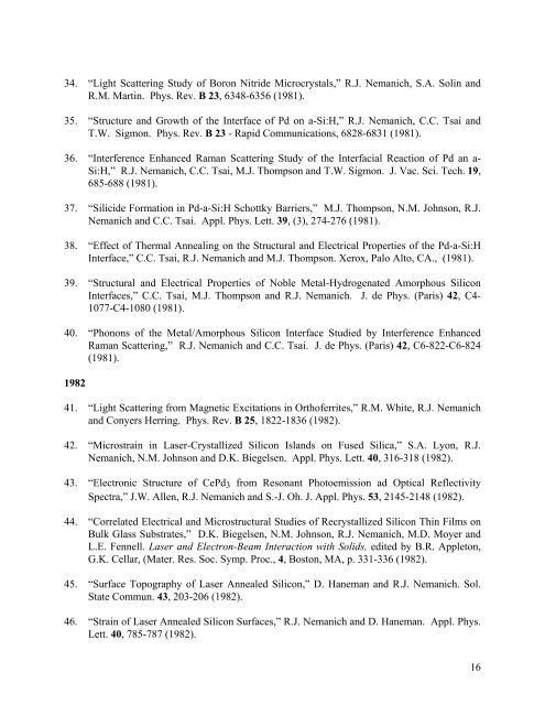
34. “Light Scattering Study <strong>of</strong> Boron Nitride Microcrystals,” R.J. Nemanich, S.A. Solin and<br />
R.M. Martin. Phys. Rev. B 23, 6348-6356 (1981).<br />
35. “Structure and Growth <strong>of</strong> the Interface <strong>of</strong> Pd on a-Si:H,” R.J. Nemanich, C.C. Tsai and<br />
T.W. Sigmon. Phys. Rev. B 23 - Rapid Communications, 6828-6831 (1981).<br />
36. “Interference Enhanced Raman Scattering Study <strong>of</strong> the Interfacial Reaction <strong>of</strong> Pd an a-<br />
Si:H,” R.J. Nemanich, C.C. Tsai, M.J. Thompson and T.W. Sigmon. J. Vac. Sci. Tech. 19,<br />
685-688 (1981).<br />
37. “Silicide Formation in Pd-a-Si:H Schottky Barriers,” M.J. Thompson, N.M. Johnson, R.J.<br />
Nemanich and C.C. Tsai. Appl. Phys. Lett. 39, (3), 274-276 (1981).<br />
38. “Effect <strong>of</strong> Thermal Annealing on the Structural and Electrical Properties <strong>of</strong> the Pd-a-Si:H<br />
Interface,” C.C. Tsai, R.J. Nemanich and M.J. Thompson. Xerox, Palo Alto, CA., (1981).<br />
39. “Structural and Electrical Properties <strong>of</strong> Noble Metal-Hydrogenated Amorphous Silicon<br />
Interfaces,” C.C. Tsai, M.J. Thompson and R.J. Nemanich. J. de Phys. (Paris) 42, C4-<br />
1077-C4-1080 (1981).<br />
40. “Phonons <strong>of</strong> the Metal/Amorphous Silicon Interface Studied by Interference Enhanced<br />
Raman Scattering,” R.J. Nemanich and C.C. Tsai. J. de Phys. (Paris) 42, C6-822-C6-824<br />
(1981).<br />
1982<br />
41. “Light Scattering from Magnetic Excitations in Orth<strong>of</strong>errites,” R.M. White, R.J. Nemanich<br />
and Conyers Herring. Phys. Rev. B 25, 1822-1836 (1982).<br />
42. “Microstrain in Laser-Crystallized Silicon Islands on Fused Silica,” S.A. Lyon, R.J.<br />
Nemanich, N.M. Johnson and D.K. Biegelsen. Appl. Phys. Lett. 40, 316-318 (1982).<br />
43. “Electronic Structure <strong>of</strong> CePd3 from Resonant Photoemission ad Optical Reflectivity<br />
Spectra,” J.W. Allen, R.J. Nemanich and S.-J. Oh. J. Appl. Phys. 53, 2145-2148 (1982).<br />
44. “Correlated Electrical and Microstructural Studies <strong>of</strong> Recrystallized Silicon Thin Films on<br />
Bulk Glass Substrates,” D.K. Biegelsen, N.M. Johnson, R.J. Nemanich, M.D. Moyer and<br />
L.E. Fennell. Laser and Electron-Beam Interaction with Solids, edited by B.R. Appleton,<br />
G.K. Cellar, (Mater. Res. Soc. Symp. Proc., 4, Boston, MA, p. 331-336 (1982).<br />
45. “Surface Topography <strong>of</strong> Laser Annealed Silicon,” D. Haneman and R.J. Nemanich. Sol.<br />
State Commun. 43, 203-206 (1982).<br />
46. “Strain <strong>of</strong> Laser Annealed Silicon Surfaces,” R.J. Nemanich and D. Haneman. Appl. Phys.<br />
Lett. 40, 785-787 (1982).<br />
16