biographical summary of robert j. nemanich - Department of Physics ...
biographical summary of robert j. nemanich - Department of Physics ...
biographical summary of robert j. nemanich - Department of Physics ...

You also want an ePaper? Increase the reach of your titles
YUMPU automatically turns print PDFs into web optimized ePapers that Google loves.
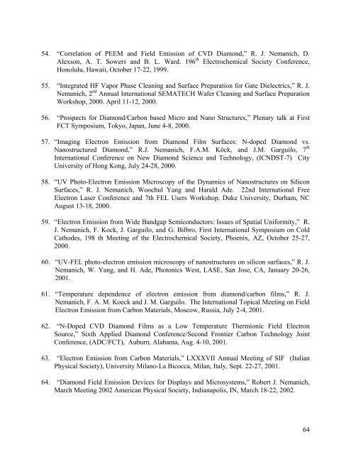
54. “Correlation <strong>of</strong> PEEM and Field Emission <strong>of</strong> CVD Diamond,” R. J. Nemanich, D.<br />
Alexson, A. T. Sowers and B. L. Ward. 196 th Electrochemical Society Conference,<br />
Honolulu, Hawaii, October 17-22, 1999.<br />
55. “Integrated HF Vapor Phase Cleaning and Surface Preparation for Gate Dielectrics,” R. J.<br />
Nemanich, 2 nd Annual International SEMATECH Wafer Cleaning and Surface Preparation<br />
Workshop, 2000. April 11-12, 2000.<br />
56. “Prospects for Diamond/Carbon based Micro and Nano Structures,” Plenary talk at First<br />
FCT Symposium, Tokyo, Japan, June 4-8, 2000.<br />
57. “Imaging Electron Emission from Diamond Film Surfaces: N-doped Diamond vs.<br />
Nanostructured Diamond,” R.J. Nemanich, F.A.M. Köck, and J.M. Garguilo, 7 th<br />
International Conference on New Diamond Science and Technology, (ICNDST-7) City<br />
University <strong>of</strong> Hong Kong, July 24-28, 2000.<br />
58. “UV Photo-Electron Emission Microscopy <strong>of</strong> the Dynamics <strong>of</strong> Nanostructures on Silicon<br />
Surfaces,” R. J. Nemanich, Woochul Yang and Harald Ade. 22nd International Free<br />
Electron Laser Conference and 7th FEL Users Workshop, Duke University, Durham, NC<br />
August 13-18, 2000.<br />
59. “Electron Emission from Wide Bandgap Semiconductors: Issues <strong>of</strong> Spatial Uniformity,” R.<br />
J. Nemanich, F. Kock, J. Garguilo, and G. Bilbro, First International Symposium on Cold<br />
Cathodes, 198 th Meeting <strong>of</strong> the Electrochemical Society, Phoenix, AZ, October 25-27,<br />
2000.<br />
60. “UV-FEL photo-electron emission microscopy <strong>of</strong> nanostructures on silicon surfaces,” R. J.<br />
Nemanich, W. Yang, and H. Ade, Photonics West, LASE, San Jose, CA, January 20-26,<br />
2001.<br />
61. “Temperature dependence <strong>of</strong> electron emission from diamond/carbon films,” R. J.<br />
Nemanich, F. A. M. Koeck and J. M. Garguilo. The International Topical Meeting on Field<br />
Electron Emission from Carbon Materials, Moscow, Russia, July 2-4, 2001.<br />
62. “N-Doped CVD Diamond Films as a Low Temperature Thermionic Field Electron<br />
Source,” Sixth Applied Diamond Conference/Second Frontier Carbon Technology Joint<br />
Conference, (ADC/FCT), Auburn, Alabama, Aug. 4-10, 2001.<br />
63. “Electron Emission from Carbon Materials,” LXXXVII Annual Meeting <strong>of</strong> SIF (Italian<br />
Physical Society), University Milano-La Bicocca, Milan, Italy, Sept. 22-27, 2001.<br />
64. “Diamond Field Emission Devices for Displays and Microsystems,” Robert J. Nemanich,<br />
March Meeting 2002 American Physical Society, Indianapolis, IN, March 18-22, 2002.<br />
64