biographical summary of robert j. nemanich - Department of Physics ...
biographical summary of robert j. nemanich - Department of Physics ...
biographical summary of robert j. nemanich - Department of Physics ...

You also want an ePaper? Increase the reach of your titles
YUMPU automatically turns print PDFs into web optimized ePapers that Google loves.
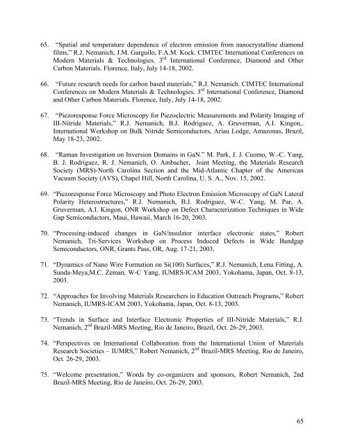
65. “Spatial and temperature dependence <strong>of</strong> electron emission from nanocrystalline diamond<br />
films,” R.J. Nemanich, J.M. Garguilo, F.A.M. Kock. CIMTEC International Conferences on<br />
Modern Materials & Technologies. 3 rd International Conference, Diamond and Other<br />
Carbon Materials. Florence, Italy, July 14-18, 2002.<br />
66. “Future research needs for carbon based materials,” R.J. Nemanich. CIMTEC International<br />
Conferences on Modern Materials & Technologies. 3 rd International Conference, Diamond<br />
and Other Carbon Materials. Florence, Italy, July 14-18, 2002.<br />
67. “Piezoresponse Force Microscopy for Piezoelectric Measurements and Polarity Imaging <strong>of</strong><br />
III-Nitride Materials,” R.J. Nemanich, B.J. Rodriguez, A. Gruverman, A.I. Kingon,.<br />
International Workshop on Bulk Nitride Semiconductors, Ariau Lodge, Amazonas, Brazil,<br />
May 18-23, 2002.<br />
68. “Raman Investigation on Inversion Domains in GaN.” M. Park, J. J. Cuomo, W.-C. Yang,<br />
B. J. Rodriguez, R. J. Nemanich, O. Ambacher, Joint Meeting, the Materials Research<br />
Society (MRS)-North Carolina Section and the Mid-Atlantic Chapter <strong>of</strong> the American<br />
Vacuum Society (AVS), Chapel Hill, North Carolina, U. S. A., Nov. 15, 2002.<br />
69. “Piezoresponse Force Microscopy and Photo Electron Emission Microscopy <strong>of</strong> GaN Lateral<br />
Polarity Heterostructures,” R.J. Nemanich, B.J. Rodriguez, W-C. Yang, M. Par, A.<br />
Gruverman, A.I. Kingon, ONR Workshop on Defect Characterization Techniques in Wide<br />
Gap Semiconductors, Maui, Hawaii, March 16-20, 2003.<br />
70. “Processing-induced changes in GaN/insulator interface electronic states,” Robert<br />
Nemanich, Tri-Services Workshop on Process Induced Defects in Wide Bandgap<br />
Semiconductors, ONR, Grants Pass, OR, Aug. 17-21, 2003.<br />
71. “Dynamics <strong>of</strong> Nano Wire Formation on Si(100) Surfaces,” R.J. Nemanich, Lena Fitting, A.<br />
Sunda-Meya,M.C. Zeman, W-C Yang, IUMRS-ICAM 2003, Yokohama, Japan, Oct. 8-13,<br />
2003.<br />
72. “Approaches for Involving Materials Researchers in Education Outreach Programs,” Robert<br />
Nemanich, IUMRS-ICAM 2003, Yokohama, Japan, Oct. 8-13, 2003.<br />
73. “Trends in Surface and Interface Electronic Properties <strong>of</strong> III-Nitride Materials,” R.J.<br />
Nemanich, 2 nd Brazil-MRS Meeting, Rio de Janeiro, Brazil, Oct. 26-29, 2003.<br />
74. “Perspectives on International Collaboration from the International Union <strong>of</strong> Materials<br />
Research Societies – IUMRS,” Robert Nemanich, 2 nd Brazil-MRS Meeting, Rio de Janeiro,<br />
Oct. 26-29, 2003.<br />
75. “Welcome presentation,” Words by co-organizers and sponsors, Robert Nemanich, 2nd<br />
Brazil-MRS Meeting, Rio de Janeiro, Oct. 26-29, 2003.<br />
65