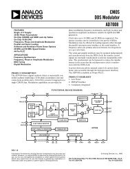
SECTION 1 SINGLE-SUPPLY AMPLIFIERS - Analog Devices
SECTION 1 SINGLE-SUPPLY AMPLIFIERS - Analog Devices
SECTION 1 SINGLE-SUPPLY AMPLIFIERS - Analog Devices
- No tags were found...

Create successful ePaper yourself
Turn your PDF publications into a flip-book with our unique Google optimized e-Paper software.
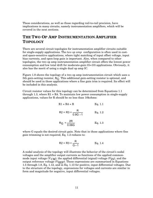
These considerations, as well as those regarding rail-to-rail precision, haveimplications in many circuits, namely instrumentation amplifiers, which will becovered in the next sections.THE TWO OP AMP INSTRUMENTATION AMPLIFIERTOPOLOGYThere are several circuit topologies for instrumentation amplifier circuits suitablefor single-supply applications. The two op amp configuration is often used in costandspace-sensitive applications, where tight matching of input offset voltage, inputbias currents, and open-loop gain is important. Also, when compared to othertopologies, the two op amp instrumentation amplifier circuit offers the lowest powerconsumption and low total drift for moderate-gain (G=10) applications. Obviously, italso has the merit of using a single dual op amp IC.Figure 1.8 shows the topology of a two op amp instrumentation circuit which uses a5th gain-setting resistor, R G . This additional gain-setting resistor is optional, andshould be used in those applications where a fine gain trim is required. Its effect willbe included in this analysis.Circuit resistor values for this topology can be determined from Equations 1.1through 1.3, where R1 = R4. To maintain low power consumption in single-supplyapplications, values for R should be no less than 10kohms:R1 = R4 = R Eq. 1.1RR2 = R3 =0.9G –1R G =2R0.06GEq. 1.2Eq. 1.3where G equals the desired circuit gain. Note that in those applications where finegain trimming is not required, Eq. 1.2 reduces to:R2 = R3 =RG–1Eq. 1.4A nodal analysis of the topology will illustrate the behavior of the circuit’s nodalvoltages and the amplifier output currents as functions of the applied commonmodeinput voltage (V CM ), the applied differential (signal) voltage (V IN ), and theoutput reference voltage (V REF ). These expressions are summarized in Equations1.5 through 1.8, Eq. 1.12, and in Eq. 1.13 for positive, input differential voltages. Dueto the structure of the topology, expressions for voltages and currents are similar inform and magnitude for negative, input differential voltages.11