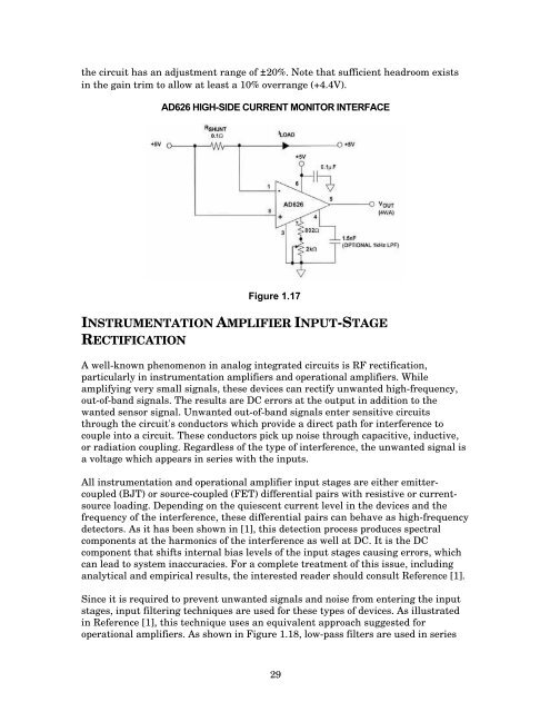
To minimize the effect of spurious RF signals at the inputs due to rectification at theinputs to A1, small filter capacitors C1 and C2, internal to the AD626, limit the inputbandwidth to 1MHz.The output of A1 is connected to the input of A2 via a 100kohm resistor (R12) toallow the low-pass filtering to the signals of interest. To use this feature, a capacitoris connected between Pin 4 and the circuit’s common. Equation 1.29 can be used todetermine the value of the capacitor, based on the corner frequency of this low-passfilter:C LP =1( Ω)2π⋅100 k ⋅fLPEq. 1.29where f LP = the desired corner frequency of the low-pass filter, in Hz.The 200kohm input impedance of the AD626 requires that the source resistancedriving this amplifier should be less than 1kohm to minimize gain error. Also, anymismatch between the total source resistance of either input will affect gainaccuracy and common-mode rejection. For example, when operating at a gain of 10,an 80ohm mismatch in the source resistance between the inputs will degrade circuitCMR to 68dB.Output amplifier, A2, operates at a gain of 2 or 20, thus setting the overall,precalibrated gain of the AD626 (with no external components) at 10 or 100. Thegain is set by the feedback network around amplifier A2.The output of A2 uses an internal 10kohm resistor to –V s to “pull down” its output.In single-supply applications where –V s equals GND, A2’s output can drive a10kohm ground-referenced load to at least +4.7V. The minimum nominal “zero”output voltage of the AD626 is 30mV.If pin 7 is left unconnected, the gain of the AD626 is 10. By connecting pin 7 to GND,the AD626’s gain can be set to 100. To adjust the gain of the AD626 for gainsbetween 10 and 100, a variable resistance network can be used between pin 7 andGND. This variable resistance network includes a fixed resistor with a rheostatconnectedpotentiometer in series. The interested reader should consult the AD626data sheet for complete details for adjusting the gain of the AD626. For theseapplications, a ±20% adjustment range in the gain is required. This is due to the onchipresistors absolute tolerance of 20% (these resistors, however, are ratiomatchedto within 0.1%).An example of the AD626 high-side sensing capabilities, Figure 1.17 illustrates atypical current sensor interface amplifier. The signal current is sensed across thecurrent shunt, R s . For reasons mentioned earlier, the value of the current shuntshould be less than 1ohm and should be selected so that the average differentialvoltage across this resistor is typically 100mV. To generate a full-scale outputvoltage of +4V, the AD626 is configured in a gain of 40. To accommodate thetolerance in the current shunt, the variable gain-setting resistor network shown in28
the circuit has an adjustment range of ±20%. Note that sufficient headroom existsin the gain trim to allow at least a 10% overrange (+4.4V).AD626 HIGH-SIDE CURRENT MONITOR INTERFACEFigure 1.17INSTRUMENTATION AMPLIFIER INPUT-STAGERECTIFICATIONA well-known phenomenon in analog integrated circuits is RF rectification,particularly in instrumentation amplifiers and operational amplifiers. Whileamplifying very small signals, these devices can rectify unwanted high-frequency,out-of-band signals. The results are DC errors at the output in addition to thewanted sensor signal. Unwanted out-of-band signals enter sensitive circuitsthrough the circuit's conductors which provide a direct path for interference tocouple into a circuit. These conductors pick up noise through capacitive, inductive,or radiation coupling. Regardless of the type of interference, the unwanted signal isa voltage which appears in series with the inputs.All instrumentation and operational amplifier input stages are either emittercoupled(BJT) or source-coupled (FET) differential pairs with resistive or currentsourceloading. Depending on the quiescent current level in the devices and thefrequency of the interference, these differential pairs can behave as high-frequencydetectors. As it has been shown in [1], this detection process produces spectralcomponents at the harmonics of the interference as well at DC. It is the DCcomponent that shifts internal bias levels of the input stages causing errors, whichcan lead to system inaccuracies. For a complete treatment of this issue, includinganalytical and empirical results, the interested reader should consult Reference [1].Since it is required to prevent unwanted signals and noise from entering the inputstages, input filtering techniques are used for these types of devices. As illustratedin Reference [1], this technique uses an equivalent approach suggested foroperational amplifiers. As shown in Figure 1.18, low-pass filters are used in series29