SECTION 1 SINGLE-SUPPLY AMPLIFIERS - Analog Devices
SECTION 1 SINGLE-SUPPLY AMPLIFIERS - Analog Devices
SECTION 1 SINGLE-SUPPLY AMPLIFIERS - Analog Devices
- No tags were found...
Create successful ePaper yourself
Turn your PDF publications into a flip-book with our unique Google optimized e-Paper software.
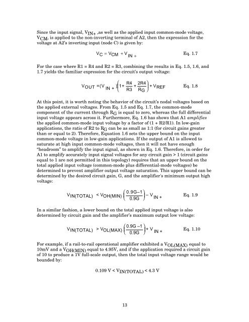
Since the input signal, V IN+ ,as well as the applied input common-mode voltage,V CM , is applied to the non-inverting terminal of A2, then the expression for thevoltage at A2’s inverting input (node C) is given by:V C= V CM + V Eq. 1.7IN +For the case where R1 = R4 and R2 = R3, combining the results in Eq. 1.5, 1.6, and1.7 yields the familiar expression for the circuit’s output voltage:V OUT =(V ) ⎛ 1+ R4IN + R3 + 2R4RG+ V REF⎝ ⎜ ⎞⎟ Eq. 1.8⎠At this point, it is worth noting the behavior of the circuit’s nodal voltages based onthe applied external voltages. From Eq. 1.5 and Eq. 1.7, the common-modecomponent of the current through R G is equal to zero, whereas the full differentialinput voltage appears across it. Furthermore, Eq. 1.6 has shows that A1 amplifiesthe applied common-mode input voltage by a factor of (1 + R2/R1). In low-gainapplications, the ratio of R2 to R G can be as small as 1:1 (for circuit gains greaterthan or equal to 2). Therefore, Equation 1.6 sets the upper bound on the inputcommon-mode voltage in low-gain applications. If the output of A1 is allowed tosaturate at high input common-mode voltages, then it will not have enough“headroom” to amplify the input signal, as shown in Eq. 1.6. Therefore, in order forA1 to amplify accurately input signal voltages for any circuit gain > 1 (circuit gainsequal to 1 are not permitted in this topology) requires that an upper bound on thetotal applied input voltage (common-mode plus differential-mode voltages) bedetermined to prevent amplifier output voltage saturation. This upper bound can bedetermined by the desired circuit gain, G, and the amplifier's minimum output highvoltage:V IN(TOTAL) < V OH(MIN)⎛ 0.9G–1⎞⎜ ⎟⎝ 0.9G – V Eq. 1.9⎠ IN +In a similar fashion, a lower bound on the total applied input voltage is alsodetermined by circuit gain and the amplifier’s maximum output low voltage:⎛ 0.9G –1 ⎞V IN(TOTAL) > V OL(MAX) ⎜ ⎟⎝ 0.9G + V Eq. 1.10⎠ IN +For example, if a rail-to-rail operational amplifier exhibited a V OL(MAX) equal to10mV and a V OH(MIN) equal to 4.95V, and if the application required a circuit gainof 10 to produce a 1V full-scale output, then the total input voltage range would bebounded by:0.109 V < V IN(TOTAL) < 4.3 V13


