SECTION 1 SINGLE-SUPPLY AMPLIFIERS - Analog Devices
SECTION 1 SINGLE-SUPPLY AMPLIFIERS - Analog Devices
SECTION 1 SINGLE-SUPPLY AMPLIFIERS - Analog Devices
- No tags were found...
You also want an ePaper? Increase the reach of your titles
YUMPU automatically turns print PDFs into web optimized ePapers that Google loves.
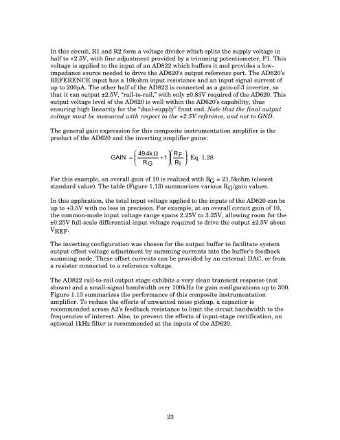
In this circuit, R1 and R2 form a voltage divider which splits the supply voltage inhalf to +2.5V, with fine adjustment provided by a trimming potentiometer, P1. Thisvoltage is applied to the input of an AD822 which buffers it and provides a lowimpedancesource needed to drive the AD620’s output reference port. The AD620’sREFERENCE input has a 10kohm input resistance and an input signal current ofup to 200µA. The other half of the AD822 is connected as a gain-of-3 inverter, sothat it can output ±2.5V, “rail-to-rail,” with only ±0.83V required of the AD620. Thisoutput voltage level of the AD620 is well within the AD620’s capability, thusensuring high linearity for the “dual-supply” front end. Note that the final outputvoltage must be measured with respect to the +2.5V reference, and not to GND.The general gain expression for this composite instrumentation amplifier is theproduct of the AD620 and the inverting amplifier gains:GAIN⎛ 49. 4kΩ ⎞= +RF⎜ ⎟ ⎛ ⎝ RG ⎠⎝ ⎜⎞1 ⎟RI ⎠Eq. 1.28For this example, an overall gain of 10 is realized with R G = 21.5kohm (closeststandard value). The table (Figure 1.13) summarizes various R G /gain values.In this application, the total input voltage applied to the inputs of the AD620 can beup to +3.5V with no loss in precision. For example, at an overall circuit gain of 10,the common-mode input voltage range spans 2.25V to 3.25V, allowing room for the±0.25V full-scale differential input voltage required to drive the output ±2.5V aboutV REF .The inverting configuration was chosen for the output buffer to facilitate systemoutput offset voltage adjustment by summing currents into the buffer’s feedbacksumming node. These offset currents can be provided by an external DAC, or froma resistor connected to a reference voltage.The AD822 rail-to-rail output stage exhibits a very clean transient response (notshown) and a small-signal bandwidth over 100kHz for gain configurations up to 300.Figure 1.13 summarizes the performance of this composite instrumentationamplifier. To reduce the effects of unwanted noise pickup, a capacitor isrecommended across A2’s feedback resistance to limit the circuit bandwidth to thefrequencies of interest. Also, to prevent the effects of input-stage rectification, anoptional 1kHz filter is recommended at the inputs of the AD620.23


