

"Linear Equation Solver using CMOS Technology" - Microelectronic ...
"Linear Equation Solver using CMOS Technology" - Microelectronic ...
"Linear Equation Solver using CMOS Technology" - Microelectronic ...

You also want an ePaper? Increase the reach of your titles
YUMPU automatically turns print PDFs into web optimized ePapers that Google loves.
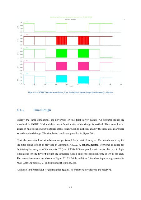
Figure 19. CADENCE Output waveforms_3 for the Revised <strong>Solver</strong> Design (4 unknowns) - 8 inputs4.1.3. Final DesignExactly the same simulations are performed on the final solver design. All possible inputs aresimulated in MODELSIM and the correct functionality of the design is verified. The circuit has noassertion misses out of 27008 applied inputs (Figure 21). In addition, exactly the same clocks are usedas in the revised design. The simulation results are provided in Figure 20.Next, the transistor level simulations are performed for a detailed analysis. The simulation setup forthe final solver design is provided in Appendix A.1.7.2. A binary2decimal converter is added forfacilitating the analysis of the outputs. 20 (out of 138) different problematic inputs observed in logicsimulations for the revised design are simulated with a transient simulation time of 10 us for each.The simulation results are shown in Figure 22, 23, 24. In addition, 55 random inputs are generated inMATLAB (Appendix 3.2) and simulated (Figure 25, 26).As shown in the transistor level simulation results, no numerical oscillations are observed.31


