Single-Chip Low Cost Low Power RF-Transceiver (Rev. A)
Single-Chip Low Cost Low Power RF-Transceiver (Rev. A)
Single-Chip Low Cost Low Power RF-Transceiver (Rev. A)

Create successful ePaper yourself
Turn your PDF publications into a flip-book with our unique Google optimized e-Paper software.
CC2500CC2500<strong>Single</strong> <strong>Chip</strong> <strong>Low</strong> <strong>Cost</strong> <strong>Low</strong> <strong>Power</strong> <strong>RF</strong> <strong>Transceiver</strong>Applications• 2400-2483.5 MHz ISM/SRD band systems• Consumer Electronics• Wireless game controllersProduct DescriptionThe CC2500 is a low cost true single chip 2.4GHz transceiver designed for very low powerwireless applications. The circuit is intendedfor the ISM (Industrial, Scientific and Medical)and SRD (Short Range Device) frequencyband at 2400-2483.5 MHz.The <strong>RF</strong> transceiver is integrated with a highlyconfigurable baseband modem. The modemsupports various modulation formats and hasa configurable data rate up to 500 kbps. Thecommunication range can be increased byenabling a Forward Error Correction option,which is integrated in the modem.CC2500 provides extensive hardware supportfor packet handling, data buffering, bursttransmissions, clear channel assessment, linkquality indication and wake-on-radio.The main operating parameters and the 64-byte transmit/receive FIFOs of CC2500 can becontrolled via an SPI interface. In a typicalsystem, the CC2500 will be used together with• Wireless audio• Wireless keyboard and mousea microcontroller and a few additional passivecomponents.CC2500 is part of <strong>Chip</strong>con’s 4 th generationtechnology platform based on 0.18 µm CMOStechnology.This data sheet contains preliminary data, and supplementary data will be published at a laterdate. <strong>Chip</strong>con reserves the right to make changes at any time without notice in order to improvedesign and supply the best possible product. The product is not fully qualified at this point.Key Features• Small size (QLP 4x4 mm package, 20pins)• True single chip 2.4 GHz <strong>RF</strong> transceiver• Frequency range: 2400-2483.5 MHz• High sensitivity (–101 dBm at 10 kbps, 1%packet error rate)• Programmable data rate up to 500 kbps• <strong>Low</strong> current consumption (13.3 mA in RX,250 kbps, input 30 dB above sensitivitylimit)• Programmable output power up to 0 dBm• Excellent receiver selectivity and blockingperformance• Very few external components:Completely on-chip frequency synthesizer,no external filters or <strong>RF</strong> switch needed• Programmable baseband modem• Ideal for multi-channel operation• Configurable packet handling hardware• Suitable for frequency hopping systemsdue to a fast settling frequency synthesizer• Optional Forward Error Correction withinterleaving• Separate 64-byte RX and TX data FIFOs• Efficient SPI interface: All registers can beprogrammed with one “burst” transfer• Digital RSSI outputPRELIMINARY Data Sheet (<strong>Rev</strong>.1.2) SWRS040A Page 1 of 83
CC2500Features (continued from front page)• Suited for systems compliant with EN 300328 and EN 300 440 class 2 (Europe),FCC CFR47 Part 15 (US), and ARIB STD-T66 (Japan)• Wake-on-radio functionality for automaticlow-power RX polling• Many powerful digital features allow ahigh-performance <strong>RF</strong> system to be madeusing an inexpensive microcontroller• Integrated analog temperature sensor• Lead-free “green“ package•• Flexible support for packet orientedsystems: On chip support for sync worddetection, address check, flexible packetlength and automatic CRC handling.• Programmable channel filter bandwidth• FSK, GFSK and MSK supported• OOK supported• Automatic Frequency Compensation(AFC) can be used to align the frequencysynthesizer to received centre frequency• Optional automatic whitening and dewhiteningof data• Support for asynchronous transparentreceive/transmit mode for backwardscompatibility with existing radiocommunication protocols• Programmable Carrier Sense indicator• Programmable Preamble Quality Indicator(PQI) for detecting preambles andimproved protection against sync worddetection in random noise• Support for automatic Clear ChannelAssessment (CCA) before transmitting (forlisten-before-talk systems)• Support for per-package Link QualityIndicationAbbreviationsAbbreviations used in this data sheet are described below.ACP Adjacent Channel <strong>Power</strong> MSK Minimum Shift KeyingADC Analog to Digital Converter NA Not ApplicableAFC Automatic Frequency Offset Compensation OOK On Off KeyingAGC Automatic Gain Control PA <strong>Power</strong> AmplifierAMR Automatic Meter Reading PCB Printed Circuit BoardARIB Association of Radio Industries and Businesses PD <strong>Power</strong> DownBER Bit Error Rate PER Packet Error RateBT Bandwidth-Time product PLL Phase Locked LoopCCA Clear Channel Assessment POR <strong>Power</strong>-on ResetCFR Code of Federal Regulations PQI Preamble Quality IndicatorCRC Cyclic Redundancy Check PQT Preamble Quality ThresholdCS Carrier Sense RCOSC RC OscillatorDC Direct Current QPSK Quadrature Phase Shift KeyingESR Equivalent Series Resistance QLP Quad Leadless PackageFCC Federal Communications Commission <strong>RF</strong> Radio FrequencyFEC Forward Error Correction RSSI Received Signal Strength IndicatorFIFO First-In-First-Out RX Receive, Receive ModeFHSS Frequency Hopping Spread Spectrum SMD Surface Mount DeviceFSK Frequency Shift Keying SNR Signal to Noise RatioGFSK Gaussian shaped Frequency Shift Keying SPI Serial Peripheral InterfaceIF Intermediate Frequency SRD Short Range DeviceI/Q In-Phase/Quadrature T/R Transmit/ReceiveISM Industrial, Scientific and Medical TX Transmit, Transmit ModeLBT Listen Before Transmit VCO Voltage Controlled OscillatorLC Inductor-Capacitor WLAN Wireless Local Area NetworksLNA <strong>Low</strong> Noise Amplifier WOR Wake on Radio, <strong>Low</strong> power pollingLO Local Oscillator XOSC Crystal OscillatorLQI Link Quality Indicator XTAL CrystalMCU Microcontroller UnitPRELIMINARY Data Sheet (<strong>Rev</strong>.1.2) SWRS040A Page 2 of 83
CC2500Table of ContentsAPPLICATIONS...........................................................................................................................................1PRODUCT DESCRIPTION.........................................................................................................................1KEY FEATURES ..........................................................................................................................................1FEATURES (CONTINUED FROM FRONT PAGE)................................................................................2ABBREVIATIONS........................................................................................................................................2TABLE OF CONTENTS ..............................................................................................................................31 ABSOLUTE MAXIMUM RATINGS..............................................................................................62 OPERATING CONDITIONS ..........................................................................................................63 GENERAL CHARACTERISTICS..................................................................................................64 ELECTRICAL SPECIFICATIONS ................................................................................................74.1 CURRENT CONSUMPTION .....................................................................................................................74.2 <strong>RF</strong> RECEIVE SECTION...........................................................................................................................84.3 <strong>RF</strong> TRANSMIT SECTION ......................................................................................................................104.4 CRYSTAL OSCILLATOR.......................................................................................................................104.5 LOW POWER RC OSCILLATOR............................................................................................................114.6 FREQUENCY SYNTHESIZER CHARACTERISTICS...................................................................................114.7 ANALOG TEMPERATURE SENSOR .......................................................................................................124.8 DC CHARACTERISTICS .......................................................................................................................124.9 POWER-ON RESET..............................................................................................................................125 PIN CONFIGURATION.................................................................................................................136 CIRCUIT DESCRIPTION .............................................................................................................157 APPLICATION CIRCUIT .............................................................................................................158 CONFIGURATION OVERVIEW.................................................................................................179 CONFIGURATION SOFTWARE.................................................................................................1810 4-WIRE SERIAL CONFIGURATION AND DATA INTE<strong>RF</strong>ACE ...........................................1910.1 CHIP STATUS BYTE ............................................................................................................................2110.2 REGISTER ACCESS..............................................................................................................................2110.3 SPI READ ...........................................................................................................................................2210.4 COMMAND STROBES ..........................................................................................................................2210.5 FIFO ACCESS .....................................................................................................................................2210.6 PATABLE ACCESS............................................................................................................................2311 MICROCONTROLLER INTE<strong>RF</strong>ACE AND PIN CONFIGURATION ...................................2311.1 CONFIGURATION INTE<strong>RF</strong>ACE..............................................................................................................2311.2 GENERAL CONTROL AND STATUS PINS ..............................................................................................2311.3 OPTIONAL RADIO CONTROL FEATURE ...............................................................................................2312 DATA RATE PROGRAMMING...................................................................................................2413 RECEIVER CHANNEL FILTER BANDWIDTH .......................................................................2414 DEMODULATOR, SYMBOL SYNCHRONIZER AND DATA DECISION............................2514.1 FREQUENCY OFFSET COMPENSATION.................................................................................................2514.2 BIT SYNCHRONIZATION......................................................................................................................2514.3 BYTE SYNCHRONIZATION...................................................................................................................2515 PACKET HANDLING HARDWARE SUPPORT .......................................................................2615.1 DATA WHITENING..............................................................................................................................2615.2 PACKET FORMAT................................................................................................................................2715.3 PACKET FILTERING IN RECEIVE MODE...............................................................................................2915.4 CRC CHECK .......................................................................................................................................2915.5 PACKET HANDLING IN TRANSMIT MODE............................................................................................2915.6 PACKET HANDLING IN RECEIVE MODE ..............................................................................................3016 MODULATION FORMATS..........................................................................................................3016.1 FREQUENCY SHIFT KEYING................................................................................................................3016.2 MINIMUM SHIFT KEYING....................................................................................................................30PRELIMINARY Data Sheet (<strong>Rev</strong>.1.2) SWRS040A Page 3 of 83
CC250016.3 AMPLITUDE MODULATION .................................................................................................................3117 RECEIVED SIGNAL QUALIFIERS AND LINK QUALITY INFORMATION .....................3117.1 SYNC WORD QUALIFIER.....................................................................................................................3117.2 PREAMBLE QUALITY THRESHOLD (PQT) ...........................................................................................3117.3 RSSI...................................................................................................................................................3117.4 CARRIER SENSE (CS)..........................................................................................................................3217.5 CLEAR CHANNEL ASSESSMENT (CCA) ..............................................................................................3317.6 LINK QUALITY INDICATOR (LQI).......................................................................................................3418 FORWARD ERROR CORRECTION WITH INTERLEAVING ..............................................3418.1 FORWARD ERROR CORRECTION (FEC)...............................................................................................3418.2 INTERLEAVING ...................................................................................................................................3419 RADIO CONTROL.........................................................................................................................3519.1 POWER-ON START-UP SEQUENCE......................................................................................................3619.2 CRYSTAL CONTROL............................................................................................................................3619.3 VOLTAGE REGULATOR CONTROL.......................................................................................................3719.4 ACTIVE MODES ..................................................................................................................................3719.5 WAKE ON RADIO (WOR)...................................................................................................................3719.6 TIMING ...............................................................................................................................................3819.7 RX TERMINATION TIMER ...................................................................................................................3820 DATA FIFO .....................................................................................................................................3921 FREQUENCY PROGRAMMING.................................................................................................402222.1VCO ..................................................................................................................................................41VCO AND PLL SELF-CALIBRATION ...................................................................................................4123 VOLTAGE REGULATORS ..........................................................................................................4124 OUTPUT POWER PROGRAMMING .........................................................................................4225 SELECTIVITY................................................................................................................................432626.1CRYSTAL OSCILLATOR.............................................................................................................45REFERENCE SIGNAL ...........................................................................................................................4627 EXTERNAL <strong>RF</strong> MATCH ..............................................................................................................4628 GENERAL PURPOSE / TEST OUTPUT CONTROL PINS ......................................................4629 ASYNCHRONOUS AND SYNCHRONOUS SERIAL OPERATION .......................................4829.1 ASYNCHRONOUS OPERATION..............................................................................................................4829.2 SYNCHRONOUS SERIAL OPERATION ....................................................................................................4830 SYSTEM CONSIDERATIONS AND GUIDELINES ..................................................................4830.1 SRD REGULATIONS............................................................................................................................4830.2 FREQUENCY HOPPING AND MULTI-CHANNEL SYSTEMS.....................................................................4930.3 WIDEBAND MODULATION NOT USING SPREAD SPECTRUM ................................................................4930.4 DATA BURST TRANSMISSIONS............................................................................................................4930.5 CONTINUOUS TRANSMISSIONS ...........................................................................................................4930.6 CRYSTAL DRIFT COMPENSATION .......................................................................................................4930.7 SPECTRUM EFFICIENT MODULATION..................................................................................................5030.8 LOW COST SYSTEMS ..........................................................................................................................5030.9 BATTERY OPERATED SYSTEMS ..........................................................................................................5030.10 INCREASING OUTPUT POWER .........................................................................................................5031 CONFIGURATION REGISTERS.................................................................................................5131.1 CONFIGURATION REGISTER DETAILS – REGISTERS WITH PRESERVED VALUES IN SLEEP STATE..........5531.2 CONFIGURATION REGISTER DETAILS – REGISTERS THAT LOSE PROGRAMMING IN SLEEP STATE ........7431.3 STATUS REGISTER DETAILS.................................................................................................................7532 PACKAGE DESCRIPTION (QLP 20)..........................................................................................7832.1 RECOMMENDED PCB LAYOUT FOR PACKAGE (QLP 20) .....................................................................7932.2 PACKAGE THERMAL PROPERTIES........................................................................................................7932.3 SOLDERING INFORMATION..................................................................................................................7932.4 TRAY SPECIFICATION..........................................................................................................................7932.5 CARRIER TAPE AND REEL SPECIFICATION ...........................................................................................80PRELIMINARY Data Sheet (<strong>Rev</strong>.1.2) SWRS040A Page 4 of 83
CC250033 ORDERING INFORMATION.......................................................................................................8034 GENERAL INFORMATION.........................................................................................................8034.1 DOCUMENT HISTORY .........................................................................................................................8034.2 PRODUCT STATUS DEFINITIONS .........................................................................................................8135 ADDRESS INFORMATION..........................................................................................................8236 TI WORLDWIDE TECHNICAL SUPPORT...............................................................................82PRELIMINARY Data Sheet (<strong>Rev</strong>.1.2) SWRS040A Page 5 of 83
CC25001 Absolute Maximum RatingsUnder no circumstances must the absolute maximum ratings given in Table 1 be violated. Stressexceeding one or more of the limiting values may cause permanent damage to the device.Caution! ESD sensitive device.Precaution should be used when handlingthe device in order to prevent permanentdamage.Parameter Min Max Units ConditionSupply voltage –0.3 3.6 V All supply pins must have the same voltageVoltage on any digital pin –0.3 VDD+0.3,max 3.6VVoltage on the pins <strong>RF</strong>_P, <strong>RF</strong>_Nand DCOUPL–0.3 2.0 VVoltage ramp-up rate 120 kV/µsInput <strong>RF</strong> level +10 dBmStorage temperature range –50 150 °CSolder reflow temperature 260 °C According to IPC/JEDEC J-STD-020CESD
CC25004 Electrical Specifications4.1 Current ConsumptionTc = 25°C, VDD = 3.0 V if nothing else stated. All measurement results obtained using the CC2500EM reference design.Parameter Min Typ Max Unit ConditionCurrent consumption inpower down modes400 nA Voltage regulator to digital part off, register values retained(SLEEP state)900 nA Voltage regulator to digital part off, register values retained, lowpowerRC oscillator running (SLEEP state with WOR enabled)92 µA Voltage regulator to digital part off, register values retained,XOSC running (SLEEP state with MCSM0.OSC_FORCE_ON set)160 µA Voltage regulator to digital part on, all other modules in powerdown (XOFF state)Current consumption8.1 µA Automatic RX polling once each second, using low-power RCoscillator, with 460 kHz filter bandwidth and 250 kbps data rate,PLL calibration every 4 th wakeup. Average current with signal inchannel below carrier sense level.35 µA Same as above, but with signal in channel above carrier senselevel, 1.9 ms RX timeout, and no preamble/sync word found.1.4 µA Automatic RX polling every 15 th second, using low-power RCoscillator, with 460 kHz filter bandwidth and 250 kbps data rate,PLL calibration every 4 th wakeup. Average current with signal inchannel below carrier sense level.42 µA Same as above, but with signal in channel above carrier senselevel, 37 ms RX timeout, and no preamble/sync word found.1.5 mA Only voltage regulator to digital part and crystal oscillator running(IDLE state)7.4 mA Only the frequency synthesizer running (after going from IDLEuntil reaching RX or TX states, and frequency calibration states)Current consumption,RX states15.3 mA Receive mode, 2.4 kbps, input at sensitivity limit,MDMCFG2.DEM_DCFILT_OFF = 112.8 mA Receive mode, 2.4 kbps, input 30 dB above sensitivity limit,MDMCFG2.DEM_DCFILT_OFF = 115.4 mA Receive mode, 10 kbps, input at sensitivity limit,MDMCFG2.DEM_DCFILT_OFF = 112.9 mA Receive mode, 10 kbps, input 30 dB above sensitivity limit,MDMCFG2.DEM_DCFILT_OFF = 118.8 mA Receive mode, 250 kbps, input at sensitivity limit,MDMCFG2.DEM_DCFILT_OFF = 015.7 mA Receive mode, 250 kbps, input 30 dB above sensitivity limit,MDMCFG2.DEM_DCFILT_OFF = 016.6 mA Receive mode, 250 kbps current optimized, input at sensitivitylimit, MDMCFG2.DEM_DCFILT_OFF = 113.3 mA Receive mode, 250 kbps current optimized, input 30 dB abovesensitivity limit, MDMCFG2.DEM_DCFILT_OFF = 119.6 mA Receive mode, 500 kbps, input at sensitivity limit,MDMCFG2.DEM_DCFILT_OFF = 017.0 mA Receive mode, 500 kbps, input 30 dB above sensitivity limit,MDMCFG2.DEM_DCFILT_OFF = 0PRELIMINARY Data Sheet (<strong>Rev</strong>.1.2) SWRS040A Page 7 of 83
CC2500Current consumption,TX states11.1 mA Transmit mode, –12 dBm output power15.1 mA Transmit mode, -6 dBm output power21.2 mA Transmit mode, 0 dBm output powerTable 4: Current consumption4.2 <strong>RF</strong> Receive SectionTc = 25°C, VDD = 3.0 V if nothing else stated. All measurement results obtained using the CC2500EM reference design.Parameter Min Typ Max Unit Condition/NoteDigital channel filterbandwidth58 812 kHz User programmable. The bandwidth limits are proportionalto crystal frequency (given values assume a 26.0 MHzcrystal).2.4 kbps data rate, current optimized, MDMCFG2.DEM_DCFILT_OFF = 1(FSK, 1% packet error rate, 20 bytes packet length, 203 kHz digital channel filter bandwidth)Receiver sensitivity –104 dBm The sensitivity can be improved to typically –106 dBm bysetting MDMCFG2.DEM_DCFILT_OFF = 0 . The typicalcurrent consumption is in this case 17.0 mA at sensitivityllimit.Saturation –13 dBmAdjacent channelrejectionAlternate channelrejection23 dB Desired channel 3 dB above the sensitivity limit. 250 kHzchannel spacing31 dB Desired channel 3 dB above the sensitivity limit. 250 kHzchannel spacingSee Figure 22 for plot of selectivity versus frequency offset10 kbps data rate, current optimized, MDMCFG2.DEM_DCFILT_OFF = 1(FSK, 1% packet error rate, 20 bytes packet length, 232 kHz digital channel filter bandwidth)Receiver sensitivity –99 dBm The sensitivity can be improved to typically –101 dBm bysetting MDMCFG2.DEM_DCFILT_OFF = 0 . The typicalcurrent consumption is in this case 17.3 mA at sensitivityllimit.Saturation –9 dBmAdjacent channelrejectionAlternate channelrejection18 dB Desired channel 3 dB above the sensitivity limit. 250 kHzchannel spacing25 dB Desired channel 3 dB above the sensitivity limit. 250 kHzchannel spacingSee Figure 23 for plot of selectivity versus frequency offset250 kbps data rate, MDMCFG2.DEM_DCFILT_OFF = 0(MSK, 1% packet error rate, 20 bytes packet length, 540 kHz digital channel filter bandwidth)Receiver sensitivity –89 dBmSaturation –13 dBmAdjacent channelrejectionAlternate channelrejection21 dB Desired channel 3 dB above the sensitivity limit. 750 kHzchannel spacing30 dB Desired channel 3 dB above the sensitivity limit. 750 kHzchannel spacingSee Figure 24 for plot of selectivity versus frequency offsetPRELIMINARY Data Sheet (<strong>Rev</strong>.1.2) SWRS040A Page 8 of 83
CC2500Parameter Min Typ Max Unit Condition/Note250 kbps data rate, current optimized, MDMCFG2.DEM_DCFILT_OFF = 1(MSK, 1% packet error rate, 20 bytes packet length, 540 kHz digital channel filter bandwidth)Receiver sensitivity –87 dBmSaturation –13 dBmAdjacent channelrejectionAlternate channelrejection21 dB Desired channel 3 dB above the sensitivity limit. 750 kHzchannel spacing30 dB Desired channel 3 dB above the sensitivity limit. 750 kHzchannel spacingSee Figure 25 for plot of selectivity versus frequency offset500 kbps data rate, MDMCFG2.DEM_DCFILT_OFF = 0(MSK, 1% packet error rate, 20 bytes packet length, 812 kHz digital channel filter bandwidth)Receiver sensitivity –82 dBmSaturation –18 dBmAdjacent channelrejectionAlternate channelrejectionGeneralBlocking at ±10 MHzoffsetBlocking at ±20 MHzoffsetBlocking at ±50 MHzoffsetSpurious emissions25 MHz – 1 GHzAbove 1 GHz14 dB Desired channel 3 dB above the sensitivity limit. 1 MHzchannel spacing25 dB Desired channel 3 dB above the sensitivity limit. 1 MHzchannel spacingSee Figure 26 for plot of selectivity versus frequency offset47 dB Desired channel at –80 dBm. Compliant with ETSI EN 300440 class 2 receiver requirements.52 dB Desired channel at –80 dBm. Compliant with ETSI EN 300440 class 2 receiver requirements.54 dB Desired channel at –80 dBm. Compliant with ETSI EN 300440 class 2 receiver requirements.–57–47dBmdBmTable 5: <strong>RF</strong> receive parametersPRELIMINARY Data Sheet (<strong>Rev</strong>.1.2) SWRS040A Page 9 of 83
CC25004.3 <strong>RF</strong> Transmit SectionTc = 25°C, VDD = 3.0 V, 0 dBm if nothing else stated. All measurement results obtained using the CC2500EM referencedesign.Parameter Min Typ Max Unit Condition/NoteDifferential loadimpedanceOutput power,highest settingOutput power,lowest settingSpurious emissions25 MHz – 1 GHz47-74, 87.5-118, 174-230, 470-862 MHz1800-1900 MHzAt 2·<strong>RF</strong> and 3·<strong>RF</strong>Otherwise above 1GHz80 + j74 Ω Differential impedance as seen from the <strong>RF</strong>-port (<strong>RF</strong>_P and<strong>RF</strong>_N) towards the antenna. Follow the CC2500EMreference design available from the TI and <strong>Chip</strong>conwebsites.0 dBm Output power is programmable and is available across theentire frequency band.Delivered to a 50 Ω single-ended load via CC2500EMreference design <strong>RF</strong> matching network.–30 dBm Output power is programmable and is available across theentire frequency band.–36–54–47–41–30dBmdBmdBmdBmdBmDelivered to a 50 Ω single-ended load via CC2500EMreference design <strong>RF</strong> matching network.Restricted band in EuropeRestricted bands in USATable 6: <strong>RF</strong> transmit parameters4.4 Crystal OscillatorTc = 25°C, VDD = 3.0 V if nothing else stated.Parameter Min Typ Max Unit Condition/NoteCrystal frequency 26 26 27 MHzTolerance ±40 ppm This is the total tolerance including a) initial tolerance, b) crystalloading, c) aging and d) temperature dependence.The acceptable crystal tolerance depends on <strong>RF</strong> frequency andchannel spacing / bandwidth.ESR 100 ΩStart-up time 300 µs Measured on CC2500EM reference design.Table 7: Crystal oscillator parametersPRELIMINARY Data Sheet (<strong>Rev</strong>.1.2) SWRS040A Page 10 of 83
CC25004.5 <strong>Low</strong> <strong>Power</strong> RC OscillatorTc = 25°C, VDD = 3.0 V if nothing else stated. All measurement results obtained using the CC2500EM reference design.Parameter Min Typ Max Unit Condition/NoteCalibrated frequency 34.6 34.7 36 kHz Calibrated RC Oscillator frequency is XTALfrequency divided by 750Frequency accuracy aftercalibration+0.3-10% The RC oscillator contains an error in thecalibration routine that statistically occurs in17.3% of all calibrations performed. The givenmaximum accuracy figures account for thecalibration error. Refer also to the CC2500Errata Note.Temperature coefficient +0.4 % / °C Frequency drift when temperature changesafter calibrationSupply voltage coefficient +3 % / V Frequency drift when supply voltage changesafter calibrationInitial calibration time 2 ms When the RC Oscillator is enabled, calibrationis continuously done in the background as longas the crystal oscillator is running.Table 8: RC oscillator parameters4.6 Frequency Synthesizer CharacteristicsTc = 25°C, VDD = 3.0 V if nothing else stated. All measurement results obtained using the CC2500EM reference design.Parameter Min Typ Max Unit Condition/NoteProgrammedfrequency resolutionSynthesizer frequencytolerance<strong>RF</strong> carrier phase noise397 F XOSC /2 16 412 Hz 26-27 MHz crystal.±40 ppm Given by crystal used. Required accuracy (includingtemperature and aging) depends on frequency band andchannel bandwidth / spacing.–78 dBc/Hz @ 50 kHz offset from carrier–78 dBc/Hz @ 100 kHz offset from carrier–81 dBc/Hz @ 200 kHz offset from carrier–90 dBc/Hz @ 500 kHz offset from carrier–100 dBc/Hz @ 1 MHz offset from carrier–108 dBc/Hz @ 2 MHz offset from carrier–116 dBc/Hz @ 5 MHz offset from carrier–127 dBc/Hz @ 10 MHz offset from carrierPLL turn-on / hop time 88.4 µs Time from leaving the IDLE state until arriving in the RX,FSTXON or TX state, when not performing calibration.Crystal oscillator running.PLL RX/TX settlingtimePLL TX/RX settlingtimePLL calibration time0.699.6 µs Settling time for the 1·IF frequency step from RX to TX21.5 µs Settling time for the 1·IF frequency step from TX to RX187390.72 0.72XOSCcyclesmsTable 9: Frequency synthesizer parametersCalibration can be initiated manually, or automaticallybefore entering or after leaving RX/TX.Min/typ/max time is for 27/26/26 MHz crystal frequency.PRELIMINARY Data Sheet (<strong>Rev</strong>.1.2) SWRS040A Page 11 of 83
CC25004.7 Analog Temperature SensorThe characteristics of the analog temperature sensor are listed in Table 10 below. Note that it isnecessary to write 0xBF to the PTEST register to use the analog temperature sensor in the IDLEstate.Parameter Min Typ Max Unit Condition/NoteOutput voltage at –40°C 0.660 VOutput voltage at 0°C 0.755 VOutput voltage at +40°C 0.859 VOutput voltage at +80°C 0.958 VTemperature coefficient 2.54 mV/°C Fitted from –20°C to +80°CError in calculatedtemperature, calibratedCurrent consumptionincrease when enabled-2 * 0 2 * °C From –20°C to +80°C when using 2.54 mV / °C,after 1-point calibration at room temperature0.3 mA* The indicated minimum and maximum error with 1-point calibration is based on simulated values fortypical process parametersTable 10: Analog temperature sensor parameters4.8 DC CharacteristicsTc = 25°C if nothing else stated.Digital Inputs/Outputs Min Max Unit ConditionLogic "0" input voltage 0 0.7 VLogic "1" input voltage VDD-0.7 VDD VLogic "0" output voltage 0 0.5 V For up to 4 mA output currentLogic "1" output voltage VDD-0.3 VDD V For up to 4 mA output currentLogic "0" input current NA –50 nA Input equals 0 VLogic "1" input current NA 50 nA Input equals VDDTable 11: DC characteristics4.9 <strong>Power</strong>-On ResetWhen the power supply complies with the requirements in Table 12 below, proper <strong>Power</strong>-On-Reset functionality is guaranteed. Otherwise, the chip should be assumed to have unknown stateuntil transmitting an SRES strobe over the SPI interface. See Section 19.1 on page 36 for furtherdetails.Parameter Min Typ Max Unit Condition/Note<strong>Power</strong> ramp-up time 5 ms From 0 V until reaching 1.8 V<strong>Power</strong> off time 1 ms Minimum time between power-on and power-off.Table 12: <strong>Power</strong>-on reset requirementsPRELIMINARY Data Sheet (<strong>Rev</strong>.1.2) SWRS040A Page 12 of 83
CC25005 Pin ConfigurationSIGNDDGUARDRBIASGND20 19 18 17 16SCLK 1SO (GDO1) 2GDO2 3DVDD 4DCOUPL 515 AVDD14 AVDD13 <strong>RF</strong>_N12 <strong>RF</strong>_P11 AVDD6GDO0 (ATEST)7CSn8XOSC_Q19AVDD10XOSC_Q2GNDExposed dieattach padFigure 1: Pinout top viewNote: The exposed die attach pad must be connected to a solid ground plane as this is the mainground connection for the chip.PRELIMINARY Data Sheet (<strong>Rev</strong>.1.2) SWRS040A Page 13 of 83
CC2500Pin # Pin name Pin type Description1 SCLK Digital Input Serial configuration interface, clock input2 SO (GDO1) Digital Output Serial configuration interface, data output.Optional general output pin when CSn is high3 GDO2 Digital Output Digital output pin for general use:• Test signals• FIFO status signals• Clear Channel Indicator• Clock output, down-divided from XOSC• Serial output RX data4 DVDD <strong>Power</strong> (Digital) 1.8 - 3.6 V digital power supply for digital I/O’s and for the digital corevoltage regulator5 DCOUPL <strong>Power</strong> (Digital) 1.6 - 2.0 V digital power supply output for decoupling.NOTE: This pin is intended for use with the CC2500 only. It can not beused to provide supply voltage to other devices.6 GDO0(ATEST)Digital I/ODigital output pin for general use:• Test signals• FIFO status signals• Clear Channel Indicator• Clock output, down-divided from XOSC• Serial output RX data• Serial input TX dataAlso used as analog test I/O for prototype/production testing7 CSn Digital Input Serial configuration interface, chip select8 XOSC_Q1 Analog I/O Crystal oscillator pin 1, or external clock input9 AVDD <strong>Power</strong> (Analog) 1.8 - 3.6 V analog power supply connection10 XOSC_Q2 Analog I/O Crystal oscillator pin 211 AVDD <strong>Power</strong> (Analog) 1.8 - 3.6 V analog power supply connection12 <strong>RF</strong>_P <strong>RF</strong> I/O Positive <strong>RF</strong> input signal to LNA in receive modePositive <strong>RF</strong> output signal from PA in transmit mode13 <strong>RF</strong>_N <strong>RF</strong> I/O Negative <strong>RF</strong> input signal to LNA in receive modeNegative <strong>RF</strong> output signal from PA in transmit mode14 AVDD <strong>Power</strong> (Analog) 1.8 - 3.6 V analog power supply connection15 AVDD <strong>Power</strong> (Analog) 1.8 - 3.6 V analog power supply connection16 GND Ground (Analog) Analog ground connection17 RBIAS Analog I/O External bias resistor for reference current18 DGUARD <strong>Power</strong> (Digital) <strong>Power</strong> supply connection for digital noise isolation19 GND Ground (Digital) Ground connection for digital noise isolation20 SI Digital Input Serial configuration interface, data inputTable 13: Pinout overviewPRELIMINARY Data Sheet (<strong>Rev</strong>.1.2) SWRS040A Page 14 of 83
CC25006 Circuit DescriptionRADIO CONTROL<strong>RF</strong>_P<strong>RF</strong>_NLNAPARC OSCBIAS090ADCADCXOSCDEMODULATO<strong>RF</strong>REQSYNTHMODULATO<strong>RF</strong>EC / INTERLEAVERPACKET HANDLERRXFIFOTXFIFODIGITAL INTE<strong>RF</strong>ACE TO MCUSCLKSO (GDO1)SICSnGDO0 (ATEST)GDO2RBIAS XOSC_Q1 XOSC_Q2Figure 2: CC2500 simplified block diagramA simplified block diagram of CC2500 is shownin Figure 2.CC2500 features a low-IF receiver. Thereceived <strong>RF</strong> signal is amplified by the lownoiseamplifier (LNA) and down-converted inquadrature (I and Q) to the intermediatefrequency (IF). At IF, the I/Q signals aredigitised by the ADCs. Automatic gain control(AGC), fine channel filtering, demodulationbit/packet synchronization is performeddigitally.The transmitter part of CC2500 is based ondirect synthesis of the <strong>RF</strong> frequency.The frequency synthesizer includes acompletely on-chip LC VCO and a 90 degreesphase shifter for generating the I and Q LOsignals to the down-conversion mixers inreceive mode.A crystal is to be connected to XOSC_Q1 andXOSC_Q2. The crystal oscillator generates thereference frequency for the synthesizer, aswell as clocks for the ADC and the digital part.A 4-wire SPI serial interface is used forconfiguration and data buffer access.The digital baseband includes support forchannel configuration, packet handling anddata buffering.7 Application CircuitOnly a few external components are requiredfor using the CC2500. The recommendedapplication circuit is shown in Figure 3. Theexternal components are described in Table14, and typical values are given in Table 15.Bias resistorThe bias resistor R171 is used to set anaccurate bias current.Balun and <strong>RF</strong> matchingC122, C132, L121 and L131 form a balun thatconverts the differential <strong>RF</strong> signal on CC2500to a single-ended <strong>RF</strong> signal. C121 and C131are needed for DC blocking. Together with anappropriate LC network, the baluncomponents also transform the impedance tomatch a 50 Ω antenna (or cable). Componentvalues for the <strong>RF</strong> balun and LC network arePRELIMINARY Data Sheet (<strong>Rev</strong>.1.2) SWRS040A Page 15 of 83
CC2500easily found using the Smart<strong>RF</strong> ® Studiosoftware. Suggested values are listed in Table15. The balun and LC filter component valuesand their placement are important to keep theperformance optimized. It is highlyrecommended to follow the CC2500EMreference design.CrystalThe crystal oscillator uses an external crystalwith two loading capacitors (C81 and C101).See Section 26 on page 45 for details.<strong>Power</strong> supply decouplingThe power supply must be properly decoupledclose to the supply pins. Note that decouplingcapacitors are not shown in the applicationcircuit. The placement and the size of thedecoupling capacitors are very important toachieve the optimum performance. TheCC2500EM reference design should befollowed closely.ComponentC51C81/C101C121/C131C122/C132C123/C124L121/L131L122R171XTALDescriptionDecoupling capacitor for on-chip voltage regulator to digital partCrystal loading capacitors, see Section 26 on page 45 for details<strong>RF</strong> balun DC blocking capacitors<strong>RF</strong> balun/matching capacitors<strong>RF</strong> LC filter/matching capacitors<strong>RF</strong> balun/matching inductors (inexpensive multi-layer type)<strong>RF</strong> LC filter inductor (inexpensive multi-layer type)Resistor for internal bias current reference26-27 MHz crystal, see Section 26 on page 45 for detailsTable 14: Overview of external components (excluding supply decoupling capacitors)1.8V-3.6V power supplyR171SIDigital IntefaceSCLKSO(GDO1)GDO2(optional)C511 SCLKSI 20GND 19DGUARD 18RBIAS 17GND 162 SO (GDO1)AVDD 143 GDO24 DVDD5 DCOUPLCC2500DIE ATTACH PAD:6 GDO07 CSn8 XOSC_Q19 AVDD10 XOSC_Q2AVDD 15<strong>RF</strong>_N 13<strong>RF</strong>_P 12AVDD 11L131C131 C132C121L121C122L122C123Antenna(50 Ohm)C124GDO0(optional)CSnXTALAlternative:Folded dipole PCBantenna (no externalcomponents needed)C81C101Figure 3: Typical application and evaluation circuit (excluding supply decoupling capacitors)PRELIMINARY Data Sheet (<strong>Rev</strong>.1.2) SWRS040A Page 16 of 83
CC2500Component Value ManufacturerC51 100 nF ±10%, 0402 X5R Murata GRM15 seriesC81 27 pF ±5%, 0402 NP0 Murata GRM15 seriesC101 27 pF ±5%, 0402 NP0 Murata GRM15 seriesC121 100 pF ±5%, 0402 NP0 Murata GRM15 seriesC122 1.0 pF ±0.25 pF, 0402 NP0 Murata GRM15 seriesC123 1.8 pF ±0.25 pF, 0402 NP0 Murata GRM15 seriesC124 1.5 pF ±0.25 pF, 0402 NP0 Murata GRM15 seriesC131 100 pF ±5%, 0402 NP0 Murata GRM15 seriesC132 1.0 pF ±0.25 pF, 0402 NP0 Murata GRM15 seriesL121 1.2 nH ±0.3 nH, 0402 monolithic Murata LQG15 seriesL122 1.2 nH ±0.3 nH, 0402 monolithic Murata LQG15 seriesL131 1.2 nH ±0.3 nH, 0402 monolithic Murata LQG15 seriesR171 56 kΩ ±1%, 0402 Koa RK73 seriesXTAL 26.0 MHz surface mount crystal NDK, AT-41CD2Table 15: Bill Of Materials for the application circuitIn the CC2500EM reference design shown inFigure 4, LQG15 series inductors from Muratahave been used. Measurements have beenperformed with multi-layer inductors from othermanufacturers (e.g. Würth) and themeasurement results were the same as whenusing the Murata part.The Gerber files for the CC2500EM referencedesign are available from the TI and <strong>Chip</strong>conwebsites.Figure 4: CC2500EM reference design8 Configuration OverviewCC2500 can be configured to achieve optimumperformance for many different applications.Configuration is done using the SPI interface.The following key parameters can beprogrammed:• <strong>Power</strong>-down / power up mode• Crystal oscillator power-up / power-down• Receive / transmit mode• <strong>RF</strong> channel selection• Data rate• Modulation format• RX channel filter bandwidth• <strong>RF</strong> output power• Data buffering with separate 64-bytereceive and transmit FIFOs• Packet radio hardware support• Forward Error Correction with interleaving• Data Whitening• Wake-On-Radio (WOR)Details of each configuration register can befound in Section 31, starting on page 51.Figure 5 shows a simplified state diagram thatexplains the main CC2500 states, together withtypical usage and current consumption. Fordetailed information on controlling the CC2500state machine, and a complete state diagram,see Section 19, starting on page 35.PRELIMINARY Data Sheet (<strong>Rev</strong>.1.2) SWRS040A Page 17 of 83
CC2500Default state when the radio is notreceiving or transmitting. Typ.current consumption: 1.5mA.Used for calibrating frequencysynthesizer upfront (enteringreceive or transmit mode can Manual freq.then be done quicker). synth. calibrationTransitional state. Typ. currentconsumption: 7.4mA.SCALSIDLESPWD or wake-on-radio (WOR)IdleCSn=0CSn=0SXOFFSRX or STX or SFSTXON or wake-on-radio (WOR)SleepCrystaloscillator off<strong>Low</strong>est power mode. Mostregister values are retained.Typ. current consumption400nA, or 900nA whenwake-on-radio (WOR) isenabled.All register values areretained. Typ. currentconsumption; 0.16mA.Frequency synthesizer is on,ready to start transmitting.Transmission starts veryquickly after receiving theSTX command strobe.Typ.current consumption: 7.4mA.Frequencysynthesizer onSFSTXONFrequencysynthesizer startup,optional calibration,settlingSTXFrequency synthesizer is turned on, can optionally becalibrated, and then settles to the correct frequency.Transitional state. Typ. current consumption: 7.4mA.SRX or wake-on-radio (WOR)STXTXOFF_MODE=01SFSTXON or RXOFF_MODE=01Typ. current consumption:11.1mA at -12dBm output,15.1mA at -6dBm output,21.2mA at 0dBm output.Transmit modeSTX or RXOFF_MODE=10SRX or TXOFF_MODE=11Receive modeTyp. currentconsumption:from 13.3mA (stronginput signal) to 16.6mA(weak input signal).In FIFO-based modes,transmission is turned offand this state entered if theTX FIFO becomes empty inthe middle of a packet. Typ.current consumption: 1.5mA.TX FIFOunderflowTXOFF_MODE=00RXOFF_MODE=00Optional transitional state. Typ.current consumption: 7.4mA.Optional freq.synth. calibrationRX FIFOoverflowIn FIFO-based modes,reception is turned off andthis state entered if the RXFIFO overflows. Typ.current consumption:1.5mA.SFTXSFRXIdleFigure 5: Simplified state diagram, with typical usage and current consumption at 250 kbpsdata rate and MDMCFG2.DEM_DCFILT_OFF = 1 (current optimized)9 Configuration SoftwareCC2500 can be configured using the Smart<strong>RF</strong> ®Studio software, available for download fromhttp://www.ti.com. The Smart<strong>RF</strong> ® Studiosoftware is highly recommended for obtainingoptimum register settings, and for evaluatingperformance and functionality. A screenshot ofthe Smart<strong>RF</strong> ® Studio user interface for CC2500is shown in Figure 6.PRELIMINARY Data Sheet (<strong>Rev</strong>.1.2) SWRS040A Page 18 of 83
CC2500Figure 6: Smart<strong>RF</strong> ® Studio user interface10 4-wire Serial Configuration and Data InterfaceCC2500 is configured via a simple 4-wire SPIcompatibleinterface (SI, SO, SCLK and CSn)where CC2500 is the slave. This interface isalso used to read and write buffered data. Alladdress and data transfer on the SPI interfaceis done most significant bit first.All transactions on the SPI interface start witha header byte containing a read/write bit, aburst access bit and a 6-bit address.During address and data transfer, the CSn pin(<strong>Chip</strong> Select, active low) must be kept low. IfCSn goes high during the access, the transferwill be cancelled. The timing for the addressand data transfer on the SPI interface isshown in Figure 7 with reference to Table 16.When CSn goes low, the MCU must wait untilCC2500 SO pin goes low before starting totransfer the header byte. This indicates thatthe voltage regulator has stabilized and thecrystal is running. Unless the chip is in theSLEEP or XOFF states or an SRES commandstrobe is issued, the SO pin will always go lowimmediately after taking CSn low.Figure 8 gives a brief overview of differentregister access types possible.PRELIMINARY Data Sheet (<strong>Rev</strong>.1.2) SWRS040A Page 19 of 83
CC2500t spt cht clt sdt hdt nsSCLK:CSn:Write to register:X 0 A6 A5 A4 A3 A2 A1 A0 X D 7 D 6 D 5 D 4 D 3 D 2 D 1 D 0 XSIW W W W W W W WHi-Z S7 S 6 S 5 S4 S 3 S 2 S 1 S0 S7 S6 S5 S4 S3 S2 S1 S0 S7 Hi-ZSORead from register:X 1 A6 A5 A4 A3 A2 A1 A0XSID 7 D 6 D 5 D 4 D 3 D 2 D 1 DSO Hi-Z S7 S 6 S 5 S4 S 3 S 2 S 1 S00R R R R R R R RHi-ZFigure 7: Configuration register write and read operations (A6 is the “burst” bit)Parameter Description Min Max Unitsf SCLKSCLK frequency100 ns delay inserted between address byte and data byte (single access), or betweenaddress and data, and between each data byte (burst access).SCLK frequency, single accessNo delay between address and data byteSCLK frequency, burst accessNo delay between address and data byte, or between data bytes- 10 MHz9 MHz6.5 MHzt sp,pd CSn low to positive edge on SCLK, in power-down mode 200 - µst sp CSn low to positive edge on SCLK, in active mode 20 - nst ch Clock high 50 - nst cl Clock low 50 - nst rise Clock rise time - 5 nst fall Clock fall time - 5 nst sdSetup data (negative SCLK edge) topositive edge on SCLK(t sd applies between address and data bytes, andbetween data bytes)<strong>Single</strong> access 55 - nsBurst access 76 - nst hd Hold data after positive edge on SCLK 20 - nst ns Negative edge on SCLK to CSn high 20 - nsTable 16: SPI interface timing requirementsCSn:Command strobe(s):Read or write register(s):Read or write consecutive registers (burst):Read or write n+1 bytes from/to <strong>RF</strong> FIFO:Combinations:ADDR strobeADDR regADDRADDR strobeDATAADDR strobe ...ADDR reg DATAADDR reg n DATA n DATA n+1 DATA n+2 ...ADDR regADDR reg DATA ...FIFODATA byte 0DATA byte 1DATA byte 2 ... DATA byte n-1DATA byte nDATAADDR strobeADDR regDATA ADDR strobeADDR FIFODATA byte 0DATA byte 1 ...Figure 8: Register access typesPRELIMINARY Data Sheet (<strong>Rev</strong>.1.2) SWRS040A Page 20 of 83
CC250010.1 <strong>Chip</strong> Status ByteWhen the header byte, data byte or commandstrobe is sent on the SPI interface, the chipstatus byte is sent by the CC2500 on the SOpin. The status byte contains key statussignals, useful for the MCU. The first bit, s7, isthe CHIP_RDYn signal; this signal must go lowbefore the first positive edge of SCLK. TheCHIP_RDYn signal indicates that the crystal isrunning and the regulated digital supplyvoltage is stable.Bits 6, 5 and 4 comprise the STATE value.This value reflects the state of the chip. TheXOSC and power to the digital core is on inthe IDLE state, but all other modules are inpower down. The frequency and channelconfiguration should only be updated when thechip is in this state. The RX state will be activewhen the chip is in receive mode. Likewise, TXis active when the chip is transmitting.The last four bits (3:0) in the status byte containsFIFO_BYTES_AVAILABLE. For readoperations, the FIFO_BYTES_AVAILABLEfield contains the number of bytes available forreading from the RX FIFO. For writeoperations, the FIFO_BYTES_AVAILABLEfield contains the number of bytes free forwriting into the TX FIFO. WhenFIFO_BYTES_AVAILABLE=15, 15 or morebytes are available/free.Table 17 gives a status byte summary.Bits Name Description7 CHIP_RDYn Stays high until power and crystal have stabilized. Should always be low when usingthe SPI interface.6:4 STATE[2:0] Indicates the current main state machine modeValue State Description000 IDLE Idle state(Also reported for some transitional states insteadof SETTLING or CALIBRATE)001 RX Receive mode010 TX Transmit mode011 FSTXON Frequency synthesizer is on, ready to starttransmitting100 CALIBRATE Frequency synthesizer calibration is running101 SETTLING PLL is settling110 RXFIFO_OVE<strong>RF</strong>LOW RX FIFO has overflowed. Read out anyuseful data, then flush the FIFO with SFRX111 TXFIFO_UNDE<strong>RF</strong>LOW TX FIFO has underflowed. Acknowledge withSFTX3:0 FIFO_BYTES_AVAILABLE[3:0] The number of bytes available in the RX FIFO or free bytes in the TX FIFO(depends on the read/write-bit). If FIFO_BYTES_AVAILABLE=15, there are 15 ormore bytes in RX FIFO or 49 or less bytes in the TX FIFO.Table 17: Status byte summary10.2 Register AccessThe configuration registers of the CC2500 arelocated on SPI addresses from 0x00 to 0x2F.Table 35 on page 52 lists all configurationregisters. The detailed description of eachregister is found in Section 31.1, starting onpage 55. All configuration registers can beboth written to and read. The read/write bitcontrols if the register should be written to orread. When writing to registers, the status byteis sent on the SO pin each time a header byteor data byte is transmitted on the SI pin.When reading from registers, the status byte issent on the SO pin each time a header byte istransmitted on the SI pin.Registers with consecutive addresses can beaccessed in an efficient way by setting thePRELIMINARY Data Sheet (<strong>Rev</strong>.1.2) SWRS040A Page 21 of 83
CC2500burst bit in the address header. The addresssets the start address in an internal addresscounter. This counter is incremented by oneeach new byte (every 8 clock pulses). Theburst access is either a read or a write accessand must be terminated by setting CSn high.For register addresses in the range 0x30-0x3D, the “burst” bit is used to select betweenstatus registers and command strobes (seebelow). The status registers can only be read.Burst read is not available for status registers,so they must be read one at a time.10.3 SPI ReadWhen reading register fields over the SPIinterface while the register fields are updatedby the radio hardware (e.g. MARCSTATE orTXBYTES), there is a small, but finite,probability that a single read from the registeris being corrupt. As an example, theprobability of any single read from TXBYTESbeing corrupt, assuming the maximum datarate is used, is approximately 80 ppm. Refer tothe CC2500 Errata Note for more details.10.4 Command StrobesCommand strobes may be viewed as singlebyte instructions to CC2500. By addressing acommand strobe register, internal sequenceswill be started. These commands are used todisable the crystal oscillator, enable receivemode, enable wake-on-radio etc. The 14command strobes are listed in Table 34 onpage 51.The command strobe registers are accessedin the same way as for a register writeoperation, but no data is transferred. That is,only the R/W bit (set to 0), burst access (set to0) and the six address bits (in the range 0x30through 0x3D) are written.When writing command strobes, the statusbyte is sent on the SO pin.A command strobe may be followed by anyother SPI access without pulling CSn high.After issuing an SRES command strobe thenext command strobe can be issued when theSO pin goes low as shown in Figure 9. Thecommand strobes are executed immediately,with the exception of the SPWD and the SXOFFstrobes that are executed when CSn goeshigh.Figure 9: SRES command strobe10.5 FIFO AccessThe 64-byte TX FIFO and the 64-byte RXFIFO are accessed through the 0x3F address.When the read/write bit is zero, the TX FIFO isaccessed, and the RX FIFO is accessed whenthe read/write bit is one.The TX FIFO is write-only, while the RX FIFOis read-only.The burst bit is used to determine if FIFOaccess is single byte or a burst access. Thesingle byte access method expects addresswith burst bit set to zero and one data byte.After the data byte a new address is expected;hence, CSn can remain low. The burst accessmethod expects one address byte and thenconsecutive data bytes until terminating theaccess by setting CSn high.The following header bytes access the FIFOs:• 0x3F: <strong>Single</strong> byte access to TX FIFO• 0x7F: Burst access to TX FIFO• 0xBF: <strong>Single</strong> byte access to RX FIFO• 0xFF: Burst access to RX FIFOWhen writing to the TX FIFO, the status byte(see Section 10.1) is output for each new databyte on SO, as shown in Figure 7. This statusbyte can be used to detect TX FIFO underflowwhile writing data to the TX FIFO. Note thatthe status byte contains the number of bytesfree before writing the byte in progress to theTX FIFO. When the last byte that fits in the TXFIFO is transmitted to the SI pin, the statusbyte received concurrently on the SO pin willindicate that one byte is free in the TX FIFO.The transmit FIFO may be flushed by issuing aSFTX command strobe. Similarly, a SFRXcommand strobe will flush the receive FIFO. ASFTX or SFRX command strobe can only beissued in the IDLE, TXFIFO_UNDERLOW orRXFIFO_OVE<strong>RF</strong>LOW state. Both FIFOs areflushed when going to the SLEEP state.PRELIMINARY Data Sheet (<strong>Rev</strong>.1.2) SWRS040A Page 22 of 83
CC250010.6 PATABLE AccessThe 0x3E address is used to access thePATABLE, which is used for selecting PApower control settings. The SPI expects up toeight data bytes after receiving the address.By programming the PATABLE, controlled PApower ramp-up and ramp-down can beachieved. See Section 24 on page 42 foroutput power programming details.The PATABLE is an 8-byte table that definesthe PA control settings to use for each of theeight PA power values (selected by the 3-bitvalue FREND0.PA_POWER). The table iswritten and read from the lowest setting (0) tothe highest (7), one byte at a time. An indexcounter is used to control the access to thetable. This counter is incremented each time abyte is read or written to the table, and set tothe lowest index when CSn is high. When thehighest value is reached the counter restartsat 0.The access to the PATABLE is either singlebyte or burst access depending on the burstbit. When using burst access the index counterwill count up; when reaching 7 the counter willrestart at 0. The read/write bit controls whetherthe access is a write access (R/W=0) or a readaccess (R/W=1).If one byte is written to the PATABLE and thisvalue is to be read out then CSn must be sethigh before the read access in order to set theindex counter back to zero.Note that the content of the PATABLE is lostwhen entering the SLEEP state, except for thefirst byte (index 0).11 Microcontroller Interface and Pin ConfigurationIn a typical system, CC2500 will interface to amicrocontroller. This microcontroller must beable to:• Program CC2500 into different modes• Read and write buffered data• Read back status information via the 4-wireSPI-bus configuration interface (SI, SO,SCLK and CSn)11.1 Configuration InterfaceThe microcontroller uses four I/O pins for theSPI configuration interface (SI, SO, SCLK andCSn). The SPI is described in Section 10 onpage 19.11.2 General Control and Status PinsThe CC2500 has two dedicated configurablepins and one shared pin that can outputinternal status information useful for controlsoftware. These pins can be used to generateinterrupts on the MCU. See Section 28 onpage 46 for more details on the signals thatcan be programmed. The dedicated pins arecalled GDO0 and GDO2. The shared pin is theSO pin in the SPI interface. The default settingfor GDO1/SO is 3-state output. By selectingany other of the programming options theGDO1/SO pin will become a generic pin. WhenCSn is low, the pin will always function as anormal SO pin.In the synchronous and asynchronous serialmodes, the GDO0 pin is used as a serial TXdata input pin while in transmit mode.The GDO0 pin can also be used for an on-chipanalog temperature sensor. By measuring thevoltage on the GDO0 pin with an external ADC,the temperature can be calculated.Specifications for the temperature sensor arefound in Section 4.7 on page 12.With default PTEST register setting (0x7F) thetemperature sensor output is only availablewhen the frequency synthesizer is enabled(e.g. the MANCAL, FSTXON, RX and TXstates). It is necessary to write 0xBF to thePTEST register to use the analog temperaturesensor in the IDLE state. Before leaving theIDLE state, the PTEST register should berestored to its default value (0x7F).11.3 Optional Radio Control FeatureThe CC2500 has an optional way of controllingthe radio, by reusing SI, SCLK and CSn fromthe SPI interface. This feature allows for asimple three-pin control of the major states ofthe radio: SLEEP, IDLE, RX and TX.This optional functionality is enabled with theMCSM0.PIN_CTRL_EN configuration bit.State changes are commanded as follows:When CSn is high the SI and SCLK is set tothe desired state according to Table 18. WhenCSn goes low the state of SI and SCLK islatched and a command strobe is generatedPRELIMINARY Data Sheet (<strong>Rev</strong>.1.2) SWRS040A Page 23 of 83
CC2500internally according to the control coding. It isonly possible to change state with thisfunctionality. That means that for instance RXwill not be restarted if SI and SCLK are set toRX and CSn toggles. When CSn is low the SIand SCLK has normal SPI functionality.All pin control command strobes are executedimmediately, except the SPWD strobe, which isdelayed until CSn goes high.CSn SCLK SI Function1 X X<strong>Chip</strong> unaffected bySCLK/SI↓ 0 0 Generates SPWD strobe↓ 0 1 Generates STX strobe↓ 1 0 Generates SIDLE strobe↓ 1 1 Generates SRX strobe0SPImodeSPImodeSPI mode (wakes up intoIDLE if in SLEEP/XOFF)Table 18: Optional pin control coding12 Data Rate ProgrammingThe data rate used when transmitting, or thedata rate expected in receive is programmedby the MDMCFG3.DRATE_M and theMDMCFG4.DRATE_E configuration registers.The data rate is given by the formula below.As the formula shows, the programmed datarate depends on the crystal frequency.R( 256 + DRATE _ M )DATA=282⋅ 2DRATE _ E⋅ fXOSCThe following approach can be used to findsuitable values for a given data rate:⎢ ⎛ RDRATE _ E = ⎢log2⎜⎢⎣⎝ fDRATE _ M =fRDATA⋅ 2⋅ 2XOSC2028DATADRATE _ EXOSC⋅ 2⎞⎥⎟⎥⎠⎥⎦− 256If DRATE_M is rounded to the nearest integerand becomes 256, increment DRATE_E anduse DRATE_M=0.The data rate can be set from 1.2 kbps to 500kbps with the minimum step size of:Data ratestart[kbps]Typicaldata rate[kbps]Data ratestop [kbps]Data ratestep size[kbps]0.8 1.2/2.4 3.17 0.00623.17 4.8 6.35 0.01246.35 9.6 12.7 0.024812.7 19.6 25.4 0.049625.4 38.4 50.8 0.099250.8 76.8 101.6 0.1984101.6 153.6 203.1 0.3967203.1 250 406.3 0.7935406.3 500 500 1.5869Table 19: Data rate step size13 Receiver Channel Filter BandwidthIn order to meet different channel widthrequirements, the receiver channel filter isprogrammable. The MDMCFG4.CHANBW_E andMDMCFG4.CHANBW_M configuration registerscontrol the receiver channel filter bandwidth,which scales with the crystal oscillatorfrequency. The following formula gives therelation between the register settings and thechannel filter bandwidth:BWchannelfXOSC=8 ⋅ (4 + CHANBW_M )·2CHANBW_EThe CC2500 supports the following channelfilter bandwidths:PRELIMINARY Data Sheet (<strong>Rev</strong>.1.2) SWRS040A Page 24 of 83
CC2500MDMCFG4.MDMCFG4.CHANBW_ECHANBW_M 00 01 10 1100 812 406 203 10201 650 325 162 8110 541 270 135 6811 464 232 116 58Table 20: Channel filter bandwidths [kHz](assuming a 26 MHz crystal)For best performance, the channel filterbandwidth should be selected so that thesignal bandwidth occupies at most 80% of thechannel filter bandwidth. The channel centretolerance due to crystal accuracy should alsobe subtracted from the signal bandwidth. Thefollowing example illustrates this:With the channel filter bandwidth set to 600kHz, the signal should stay within 80% of 600kHz, which is 480 kHz. Assuming 2.44 GHzfrequency and ±20 ppm frequency uncertaintyfor both the transmitting device and thereceiving device, the total frequencyuncertainty is ±40 ppm of 2.44 GHz, which is±98 kHz. If the whole transmitted signalbandwidth is to be received within 480 kHz,the transmitted signal bandwidth should bemaximum 480 kHz – 2·98 kHz, which is 284kHz.14 Demodulator, Symbol Synchronizer and Data DecisionCC2500 contains an advanced and highlyconfigurable demodulator. Channel filteringand frequency offset compensation isperformed digitally. To generate the RSSI level(see Section 17.3 for more information) thesignal level in the channel is estimated. Datafiltering is also included for enhancedperformance.14.1 Frequency Offset CompensationWhen using FSK, GFSK or MSK modulation,the demodulator will compensate for the offsetbetween the transmitter and receiverfrequency, within certain limits, by estimatingthe centre of the received data. This value isavailable in the FREQEST status register.Writing the value from FREQEST intoFSCTRL0.FREQOFF the frequencysynthesizer is automatically adjustedaccording to the estimated frequency offset.Note that frequency offset compensation is notsupported for OOK modulation.14.2 Bit SynchronizationThe bit synchronization algorithm extracts theclock from the incoming symbols. Thealgorithm requires that the expected data rateis programmed as described in Section 12 onpage 24. Re-synchronization is performedcontinuously to adjust for error in the incomingsymbol rate.14.3 Byte SynchronizationByte synchronization is achieved by acontinuous sync word search. The sync wordis a 16 or 32 bit configurable field that isautomatically inserted at the start of the packetby the modulator in transmit mode. Thedemodulator uses this field to find the byteboundaries in the stream of bits. The syncword will also function as a system identifier,since only packets with the correct predefinedsync word will be received. The sync worddetector correlates against the user-configured16-bit sync word. The correlation thresholdcan be set to 15/16 bits match or 16/16 bitsmatch. The sync word can be further qualifiedusing the preamble quality indicatormechanism described below and/or a carriersense condition. The sync word isprogrammed with SYNC1 and SYNC0.In order to make false detections of syncwords less likely, a mechanism calledpreamble quality indication (PQI) can be usedto qualify the sync word. A threshold value forthe preamble quality must be exceeded inorder for a detected sync word to be accepted.See Section 17.2 on page 31 for more details.PRELIMINARY Data Sheet (<strong>Rev</strong>.1.2) SWRS040A Page 25 of 83
CC250015 Packet Handling Hardware SupportThe CC2500 has built-in hardware support forpacket oriented radio protocols.In transmit mode, the packet handler will addthe following elements to the packet stored inthe TX FIFO:• A programmable number of preamblebytes.• A two byte synchronization (sync) word.Can be duplicated to give a 4-byte syncword.• Optionally whiten the data with a PN9sequence.• Optionally Interleave and Forward ErrorCode the data.• Optionally compute and add a CRCchecksum over the data field.• The recommended setting is 4-bytepreamble and 4-byte sync word except for500 kbps data rate where therecommended preamble length is 8 bytes.In receive mode, the packet handling supportwill de-construct the data packet:• Preamble detection.• Sync word detection.• Optional one byte address check.• Optionally compute and check CRC.• Optionally append two status bytes (seeTable 21 and Table 22) with RSSI value,Link Quality Indication and CRC status.Bit Field name Description7:0 RSSI RSSI valueTable 21: Received packet status byte 1(first byte appended after the data)Bit Field name Description7 CRC_OK 1: CRC for received data OK (orCRC disabled)0: CRC error in received data6:0 LQI The Link Quality Indicatorestimates how easily a receivedsignal can be demodulatedTable 22: Received packet status byte 2(second byte appended after the data)Note that register fields that control the packethandling features should only be altered whenCC2500 is in the IDLE state.15.1 Data WhiteningFrom a radio perspective, the ideal over the airdata are random and DC free. This results inthe smoothest power distribution over theoccupied bandwidth. This also gives theregulation loops in the receiver uniformoperation conditions (no data dependencies).Real world data often contain long sequencesof zeros and ones. Performance can then beimproved by whitening the data beforetransmitting, and de-whitening in the receiver.With CC2500, this can be done automaticallyby setting PKTCTRL0.WHITE_DATA=1. Alldata, except the preamble and the sync word,are then XOR-ed with a 9-bit pseudo-random(PN9) sequence before being transmitted asshown in Figure 10. At the receiver end, thedata are XOR-ed with the same pseudorandomsequence. This way, the whitening isreversed, and the original data appear in thereceiver.Data whitening can only be used whenPKTCTRL0.CC2400_EN = 0 (default).PRELIMINARY Data Sheet (<strong>Rev</strong>.1.2) SWRS040A Page 26 of 83
CC2500Figure 10: Data whitening in TX mode15.2 Packet FormatThe format of the data packet can beconfigured and consists of the following items(see Figure 11):• Preamble• Synchronization word• Length byte or constant programmablepacket length• Optional address byte• Payload• Optional 2 byte CRCOptional data whiteningOptionally FEC encoded/decodedOptional CRC-16 calculationLegend:Inserted automatically in TX,processed and removed in RX.Preamble bits(1010...1010)Sync word8 x n bits 16/32 bitsLength field8bitsAddress field8bitsData fieldCRC-168 x n bits 16 bitsFigure 11: Packet formatOptional user-provided fields processed in TX,processed but not removed in RX.Unprocessed user data (apart from FECand/or whitening)The preamble pattern is an alternatingsequence of ones and zeros (01010101…).The minimum length of the preamble isprogrammable. When enabling TX, themodulator will start transmitting the preamble.When the programmed number of preamblebytes has been transmitted, the modulator willsend the sync word and then data from the TXFIFO if data is available. If the TX FIFO isempty, the modulator will continue to sendpreamble bytes until the first byte is written tothe TX FIFO. The modulator will then send thesync word and then the data bytes. Thenumber of preamble bytes is programmed withthe MDMCFG1.NUM_PREAMBLE value.The synchronization word is a two-byte valueset in the SYNC1 and SYNC0 registers. Thesync word provides byte synchronization of theincoming packet. A one-byte sync word can beemulated by setting the SYNC1 value to thepreamble pattern. It is also possible to emulatea 32 bit sync word by usingMDMCFG2.SYNC_MODE=3 or 7. The sync wordwill then be repeated twice.CC2500 supports both fixed packet lengthprotocols and variable packet length protocols.Variable or fixed packet length mode can beused for packets up to 255 bytes. For longerpackets, infinite packet length mode must beused.PRELIMINARY Data Sheet (<strong>Rev</strong>.1.2) SWRS040A Page 27 of 83
CC2500Fixed packet length mode is selected bysetting PKTCTRL0.LENGTH_CONFIG=0. Thedesired packet length is set by the PKTLENregister.In variable packet length mode,PKTCTRL0.LENGTH_CONFIG=1, the packetlength is configured by the first byte after thesync word. The packet length is defined as thepayload data, excluding the length byte andthe optional automatic CRC. The PKTLENregister is used to set the maximum packetlength allowed in RX. Any packet received witha length byte with a value greater thanPKTLEN will be discarded.With PKTCTRL0.LENGTH_CONFIG=2, thepacket length is set to infinite and transmissionand reception will continue until turned offmanually. The infinite mode can be turned offwhile a packet is being transmitted or received.As described in the next section, this can beused to support packet formats with differentlength configuration than natively supported byCC2500.15.2.1 Arbitrary Length Field ConfigurationThe fixed length field can be reprogrammedduring receive and transmit. This opens thepossibility to have a different length fieldconfiguration than supported for variablelength packets. At the start of reception, thepacket length is set to a large value. The MCUreads out enough bytes to interpret the lengthfield in the packet. Then the PKTLEN value isset according to this value. The end of packetwill occur when the byte counter in the packethandler is equal to the PKTLEN register. Thus,the MCU must be able to program the correctlength, before the internal counter reaches thepacket length.By utilizing the infinite packet length option,arbitrary packet length is available. At the startof the packet, the infinite mode must be active.On the TX side, the PKTLEN register is set tomod(length, 256). On the RX side theMCU reads out enough bytes to interpret thelength field in the packet and sets the PKTLENregister to mod(length, 256). When lessthan 256 bytes remains of the packet the MCUdisables infinite packet length and activatesfixed length packets. When the internal bytecounter reaches the PKTLEN value, thetransmission or reception ends. AutomaticCRC appending/checking can be used (bysetting PKTCTRL0.CRC_EN to 1).When for example a 600-byte packet is to betransmitted, the MCU should do the following(see also Figure 12):• Set PKTCTRL0.LENGTH_CONFIG=2 (10).• Pre-program the PKTLEN register tomod(600,256)=88.• Transmit at least 345 bytes, for exampleby filling the 64-byte TX FIFO six times(384 bytes transmitted).• Set PKTCTRL0.LENGTH_CONFIG=0 (00).• The transmission ends when the packetcounter reaches 88. A total of 600 bytesare transmitted.Internal byte counter in packet handler counts from 0 to 255 and then starts at 0 again0,1,..........,88,....................255,0,........,88,..................,255,0,........,88,..................,255,0,.......................Infinite packet length enabledFixed packet lengthenabled when less than256 bytes remains ofpacketLength field transmitted and received. Rx and Tx PKTLEN value set to mod(600,256) = 88Figure 12: Arbitrary length field configuration600 bytes transmitted andreceivedPRELIMINARY Data Sheet (<strong>Rev</strong>.1.2) SWRS040A Page 28 of 83
CC250015.3 Packet Filtering in Receive ModeCC2500 supports three different packet-filteringcriteria: address filtering, maximum lengthfiltering and CRC filtering.15.3.1 Address FilteringSetting PKTCTRL1.ADR_CHK to any othervalue than zero enables the packet addressfilter. The packet handler engine will comparethe destination address byte in the packet withthe programmed node address in the ADDRregister and the 0x00 broadcast address whenPKTCTRL1.ADR_CHK=10 or both 0x00 and0xFF broadcast addresses whenPKTCTRL1.ADR_CHK=11. If the receivedaddress matches a valid address, the packet isreceived and written into the RX FIFO. If theaddress match fails, the packet is discardedand receive mode restarted (regardless of theMCSM1.RXOFF_MODE setting).If the received address matches a validaddress when the packet length is set toinfinite and address filtering is enabled, 0xFFwill be written into the RX FIFO followed by theaddress byte and then the payload data.15.3.2 Maximum Length FilteringIn the variable packet length mode thePKTLEN.PACKET_LENGTH register value isused to set the maximum allowed packetlength. If the received length byte has a largervalue than this, the packet is discarded andreceive mode restarted (regardless of theMCSM1.RXOFF_MODE setting).15.3.3 CRC FilteringThe filtering of a packet when CRC check failsis enabled with PKTCTRL1.CRC_AUTOFLUSH.The CRC auto flush function will flush theentire RX FIFO if the CRC check fails. Afterauto flushing the RX FIFO, the next statedepends on the MCSM1.RXOFF_MODE setting.PKTCTRL0.CC2400_EN must be 0 (default)for the CRC auto flush function to workcorrectly.When using the auto flush function, themaximum packet length is 63 bytes in variablepacket length mode and 64 bytes in fixedpacket length mode. Note that the maximumallowed packet length is reduced by two byteswhen PKTCTRL1.APPEND_STATUS isenabled, to make room in the RX FIFO for thetwo status bytes appended at the end of thepacket. Since the entire RX FIFO is flushedwhen the CRC check fails, the previouslyreceived packet must be read out of the FIFObefore receiving the current packet. The MCUmust not read from the current packet until theCRC has been checked as OK.15.4 CRC CheckThere are two different CRC implementations.PKTCTRL0.CC2400_EN selects between the2 options. The CRC check is different for the 2options. Refer also to the CC2500 Errata Note.15.4.1 PKTCTRL0.CC2400_EN = 0If PKTCTRL0.CC2400_EN =0 it is possible toread back the CRC status in 2 different ways:1) Set PKTCTRL1.APPEND_STATUS=1 andread the CRC_OK flag in the MSB of thesecond byte appended to the RX FIFO afterthe packet data. This requires double bufferingof the packet, i.e. the entire packet content ofthe RX FIFO must be completely read outbefore it is possible to check whether the CRCindication is OK or not.2) To avoid reading the entire RX FIFO,another solution is to use thePKTCTRL1.CRC_AUTOFLUSH feature. If thisfeature is enabled, the entire RX FIFO will beflushed if the CRC check fails. IfGDOx_CFG=0x06 the GDOx pin will beasserted when a sync word is found. TheGDOx pin will be de-asserted at the end of thepacket. When the latter occurs the MCUshould read the number of bytes in the RXFIFO from the RXBYTES.NUM_RXBYTESstatus register. If RXBYTES.NUM_RXBYTES=0the CRC check failed and the FIFO is flushed.If RXBYTES.NUM_RXBYTES>0 the CRC checkwas OK and data can be read out of the FIFO.15.4.2 PKTCTRL0.CC2400_EN = 1If PKTCTRL0.CC2400_EN = 1 the CRC can bechecked as outlined in 1) in Section 15.4.1 aswell as by reading the CRC_OK flag availablein the PKTSTATUS[7] register, in the LQI[7]status register or from one of the GDO pins ifGDOx_CFG is 0x07 or 0x15.The PKTCTRL1.CRC_AUTOFLUSH or datawhitening cannot be used whenPKTCTRL0.CC2400_EN = 1.15.5 Packet Handling in Transmit ModeThe payload that is to be transmitted must bewritten into the TX FIFO. The first byte writtenmust be the length byte when variable packetPRELIMINARY Data Sheet (<strong>Rev</strong>.1.2) SWRS040A Page 29 of 83
CC2500length is enabled. The length byte has a valueequal to the payload of the packet (includingthe optional address byte). If fixed packetlength is enabled, then the first byte written tothe TX FIFO is interpreted as the destinationaddress, if this feature is enabled in the devicethat receives the packet.The modulator will first send the programmednumber of preamble bytes. If data is availablein the TX FIFO, the modulator will send thetwo-byte (optionally 4-byte) sync word andthen the payload in the TX FIFO. If CRC isenabled, the checksum is calculated over allthe data pulled from the TX FIFO and theresult is sent as two extra bytes at the end ofthe payload data.If whitening is enabled, the length byte,payload data and the two CRC bytes will bewhitened. This is done before the optionalFEC/Interleaver stage. Whitening is enabledby setting PKTCTRL0.WHITE_DATA=1.If FEC/Interleaving is enabled, the length byte,payload data and the two CRC bytes will bescrambled by the interleaver, and FECencoded before being modulated.15.6 Packet Handling in Receive ModeIn receive mode, the demodulator and packethandler will search for a valid preamble andthe sync word. When found, the demodulatorhas obtained both bit and byte synchronismand will receive the first payload byte.If FEC/Interleaving is enabled, the FECdecoder will start to decode the first payloadbyte. The interleaver will de-scramble the bitsbefore any other processing is done to thedata.If whitening is enabled, the data will be dewhitenedat this stage.When variable packet length is enabled, thefirst byte is the length byte. The packet handlerstores this value as the packet length andreceives the number of bytes indicated by thelength byte. If fixed packet length is used, thepacket handler will accept the programmednumber of bytes.Next, the packet handler optionally checks theaddress and only continues the reception if theaddress matches. If automatic CRC check isenabled, the packet handler computes CRCand matches it with the appended CRCchecksum.At the end of the payload, the packet handlerwill optionally write two extra packet statusbytes that contain CRC status, link qualityindication and RSSI value.16 Modulation FormatsCC2500 supports amplitude, frequency andphase shift modulation formats. The desiredmodulation format is set in theMDMCFG2.MOD_FORMAT register.Optionally, the data stream can be Manchestercoded by the modulator and decoded by thedemodulator. This option is enabled by settingMDMCFG2.MANCHESTER_EN=1. Manchesterencoding is not supported at the same time asusing the FEC/Interleaver option.16.1 Frequency Shift KeyingFSK can optionally be shaped by a Gaussianfilter with BT=1, producing a GFSK modulatedsignal.The frequency deviation is programmed withthe DEVIATION_M and DEVIATION_E valuesin the DEVIATN register. The value has anexponent/mantissa form, and the resultantdeviation is given by:fdevf=2xoscDEVIATION _ E⋅ (8 + DEVIATION _ M ) ⋅ 217The symbol encoding is shown in Table 23.Format Symbol CodingFSK\GFSK ‘0’ – Deviation‘1’ + DeviationTable 23: Symbol encoding for FSKmodulation16.2 Minimum Shift KeyingWhen using MSK 1 , the complete transmission(preamble, sync word and payload) will beMSK modulated.1Identical to offset QPSK with half-sineshaping (data coding may differ)PRELIMINARY Data Sheet (<strong>Rev</strong>.1.2) SWRS040A Page 30 of 83
CC2500Phase shifts are performed with a constanttransition time.The fraction of a symbol period used tochange the phase can be modified with theDEVIATN.DEVIATION_M setting. This isequivalent to changing the shaping of thesymbol.The MSK modulation format implemented inCC2500 inverts the sync word and datacompared to e.g. signal generators.16.3 Amplitude ModulationThe supported amplitude modulation On-OffKeying (OOK) simply turns on or off the PA tomodulate 1 and 0 respectively.17 Received Signal Qualifiers and Link Quality InformationCC2500 has several qualifiers that can be usedto increase the likelihood that a valid syncword is detected.17.1 Sync Word QualifierIf sync word detection in RX is enabled inregister MDMCFG2 the CC2500 will not startfilling the RX FIFO and perform the packetfiltering described in Section 15.3 before avalid sync word has been detected. The syncword qualifier mode is set byMDMCFG2.SYNC_MODE and is summarized inTable 24. Carrier sense in Table 24 isdescribed in Section 17.4.MDMCFG2.SYNC_MODESync word qualifier mode000 No preamble/sync001 15/16 sync word bits detected010 16/16 sync word bits detected011 30/32 sync word bits detected100 No preamble/sync, carrier senseabove threshold101 15/16 + carrier sense above threshold110 16/16 + carrier sense above threshold111 30/32 + carrier sense above thresholdTable 24: Sync word qualifier mode17.2 Preamble Quality Threshold (PQT)The Preamble Quality Threshold (PQT) syncwordqualifier adds the requirement that thereceived sync word must be preceded with apreamble with a quality above a programmedthreshold.Another use of the preamble quality thresholdis as a qualifier for the optional RX terminationtimer. See Section 19.7 on page 38 for details.The preamble quality estimator increases aninternal counter by one each time a bit isreceived that is different from the previous bit,and decreases the counter by 4 each time abit is received that is the same as the last bit.The counter saturates at 0 and 31. Thethreshold is configured with the register fieldPKTCTRL1.PQT. A threshold of 4·PQT for thiscounter is used to gate sync word detection.By setting the value to zero, the preamblequality qualifier of the sync word is disabled.A “Preamble Quality Reached” flag can alsobe observed on one of the GDO pins and inthe status register bitPKTSTATUS.PQT_REACHED. This flag assertswhen the received signal exceeds the PQT.17.3 RSSIThe RSSI value is an estimate of the signallevel in the chosen channel. This value isbased on the current gain setting in the RXchain and the measured signal level in thechannel.In RX mode, the RSSI value can be readcontinuously from the RSSI status registeruntil the demodulator detects a sync word(when sync word detection is enabled). At thatpoint the RSSI readout value is frozen until thenext time the chip enters the RX state. TheRSSI value is in dB with ½dB resolution. TheRSSI update rate depends on the receiverfilter bandwidth (BW channel defined in Section13) and AGCCTRL0.FILTER_LENGTH.fRSSI2 ⋅ BW=8⋅2channelFILTER _ LENGTHPRELIMINARY Data Sheet (<strong>Rev</strong>.1.2) SWRS040A Page 31 of 83
CC2500If PKTCTRL1.APPEND_STATUS is enabled theRSSI value at sync word detection isautomatically added to the first byte appendedafter the data.The RSSI value read from the RSSI statusregister is a 2’s complement number. Thefollowing procedure can be used to convert theRSSI reading to an absolute power level(RSSI_dBm).1) Read the RSSI status register2) Convert the reading from a hexadecimalnumber to a decimal number (RSSI_dec)3) If RSSI_dec ≥ 128 then RSSI_dBm =(RSSI_dec - 256)/2 – RSSI_offset4) Else if RSSI_dec < 128 then RSSI_dBm =(RSSI_dec)/2 – RSSI_offsetTable 25 provides typical values for theRSSI_offset.Figure 13 shows typical plots of RSSI readingsas a function of input power level for differentdata rates.Data rate[kbps]RSSI_offset [decimal]2.4 7110 69250 72500 72Table 25: Typical RSSI_offset values0.0-10.0-20.0-30.0RSSI readout [dBm]-40.0-50.0-60.0-70.0-80.0-90.0-100.0-110.0-120.0-120 -110 -100 -90 -80 -70 -60 -50 -40 -30 -20 -10 0Input power [dBm]2.4 kbps 10 kbps 250 kbps 250 kbps, reduced current 500 kbpsFigure 13: Typical RSSI value vs. input power level for some typical data rates17.4 Carrier Sense (CS)The Carrier Sense flag is used as a sync wordqualifier and for CCA. The CS flag can be setbased on two conditions, which can beindividually adjusted:• CS is asserted when the RSSI is above aprogrammable absolute threshold, and deassertedwhen RSSI is below the samethreshold (with hysteresis).• CS is asserted when the RSSI hasincreased with a programmable number ofdB from one RSSI sample to the next, andde-asserted when RSSI has decreasedwith the same number of dB. This settingis not dependent on the absolute signallevel and is thus useful to detect signals inenvironments with a time varying noisefloor.PRELIMINARY Data Sheet (<strong>Rev</strong>.1.2) SWRS040A Page 32 of 83
CC2500Carrier Sense (CS) can be used as a syncword qualifier that requires the signal level tobe higher than the threshold for a sync wordsearch to be performed. The signal can alsobe observed on one of the GDO pins and inthe status register bit PKTSTATUS.CS.Other uses of Carrier Sense include the TX-If-CCA function (see Section 17.5 on page 33)and the optional fast RX termination (seeSection 19.7 on page 38).CS can be used to avoid interference from e.g.WLAN.17.4.1 CS Absolute ThresholdThe absolute threshold related to the RSSIvalue is given by:THRRSSI= MAGN _ TARGET +CARRIER _ SENSE _ ABS _ THR − GAINMAXThe maximum possible gain can be reducedusing the AGCCTRL2.MAX_LNA_GAIN andAGCCTRL2.MAX_DVGA_GAIN register fields.CARRIER_SENSE_ABS_THR is programmablein 1 dB steps from -7 dB to + 7dB. Table 26and Table 27 show the RSSI readout valuesat the CS threshold at 2.4 kbps and 250 kbpsdata rate respectively. The defaultCARRIER_SENSE_ABS_THR = 0 (0 dB) andMAGN_TARGET = 3 (33 dB) have been used.MAX_LNA_GAIN[2:0]MAX_DVGA_GAIN[1:0]00 01 10 11000 -96 -90 -84 -78.5001 -94.5 -89 -83 -77.5010 -92.5 -87 -81 -75011 -91 -85 -78.5 -73100 -87.5 -82 -76 -70101 -85 -79.5 -73.5 -67.5110 -83 -76.5 -70.5 -65111 -78 -72 -66 -60Table 27: Typical RSSI value in dBm at CSthreshold with default MAGN_TARGET at250 kbpsIf the threshold is set high, i.e. only strongsignals are wanted, the threshold should beadjusted upwards by first reducing theMAX_LNA_GAIN value and then theMAX_DVGA_GAIN value. This will reducepower consumption in the receiver front end,since the highest gain settings are avoided.The MAGN_TARGET setting is a compromisebetween blocker tolerance/selectivity andsensitivity. The value sets the desired signallevel in the channel into the demodulator.Increasing this value reduces the headroomfor blockers, and therefore close-in selectivity.MAX_LNA_GAIN[2:0]MAX_DVGA_GAIN[1:0]00 01 10 11000 -99 -93 -87 -81.5001 -97 -90.5 -85 -78.5010 -93.5 -87 -82 -76011 -91.5 -86 -80 -74100 -90.5 -84 -78 -72.5101 -88 -82.5 -76 -70110 -84.5 -78.5 -73 -67111 -82.5 -76 -70 -64Table 26: Typical RSSI value in dBm at CSthreshold with default MAGN_TARGET at 2.4kbps17.4.2 CS relative thresholdThe relative threshold detects sudden changesin the measured signal level. This setting is notdependent on the absolute signal level and isthus useful to detect signals in environmentswith a time varying noise floor. The registerfield AGCCTRL1.CARRIER_SENSE_REL_THRis used to enable/disable relative CS, and toselect threshold of 6 dB, 10 dB or 14 dB RSSIchange17.5 Clear Channel Assessment (CCA)The Clear Channel Assessment is used toindicate if the current channel is free or busy.The current CCA state is viewable on any ofthe GDO pins.MCSM1.CCA_MODE selects the mode to usewhen determining CCA.When the STX or SFSTXON command strobe isgiven while CC2500 is in the RX state, the TXstate is only entered if the clear channelrequirements are fulfilled. The chip willPRELIMINARY Data Sheet (<strong>Rev</strong>.1.2) SWRS040A Page 33 of 83
CC2500otherwise remain in RX. This feature is calledTX if CCA.Four CCA requirements can be programmed:• Always (CCA disabled, always goes to TX)• If RSSI is below threshold• Unless currently receiving a packet• Both the above (RSSI below threshold andnot currently receiving a packet)17.6 Link Quality Indicator (LQI)The Link Quality Indicator is a metric of thecurrent quality of the received signal. IfPKTCTRL1.APPEND_STATUS is enabled, thevalue is automatically appended to the end ofeach received packet. The value can also beread from the LQI status register. The LQI iscalculated over the 64 symbols following thesync word (first 8 packet bytes). LQI is bestused as a relative measurement of the linkquality, since the value is dependent on themodulation format.18 Forward Error Correction with Interleaving18.1 Forward Error Correction (FEC)CC2500 has built in support for Forward ErrorCorrection (FEC). To enable this option, setMDMCFG1.FEC_EN to 1. FEC is only supportedin fixed packet length mode(PKTCTRL0.LENGTH_CONFIG=0). FEC isemployed on the data field and CRC word inorder to reduce the gross bit error rate whenoperating near the sensitivity limit.Redundancy is added to the transmitted datain such a way that the receiver can restore theoriginal data in the presence of some biterrors.The use of FEC allows correct reception at alower SNR, thus extending communicationrange. Alternatively, for a given SNR, usingFEC decreases the bit error rate (BER). As thepacket error rate (PER) is related to BER by:PER = 1−(1 − BER)packet _ lengtha lower BER can be used to allow longerpackets, or a higher percentage of packets ofa given length, to be transmitted successfully.Finally, in realistic ISM radio environments,transient and time-varying phenomena willproduce occasional errors even in otherwisegood reception conditions. FEC will mask sucherrors and, combined with interleaving of thecoded data, even correct relatively longperiods of faulty reception (burst errors).The FEC scheme adopted for CC2500 isconvolutional coding, in which n bits aregenerated based on k input bits and the mmost recent input bits, forming a code streamable to withstand a certain number of bit errorsbetween each coding state (the m-bit window).The convolutional coder is a rate 1/2 code witha constraint length of m=4. The coder codesone input bit and produces two output bits;hence, the effective data rate is halved.18.2 InterleavingData received through radio channels willoften experience burst errors due tointerference and time-varying signal strengths.In order to increase the robustness to errorsspanning multiple bits, interleaving is usedwhen FEC is enabled. After de-interleaving, acontinuous span of errors in the receivedstream will become single errors spread apart.CC2500 employs matrix interleaving, which isillustrated in Figure 14. The on-chipinterleaving and de-interleaving buffers are 4 x4 matrices. In the transmitter, the data bits arewritten into the rows of the matrix, whereas thebit sequence to be transmitted is read from thecolumns of the matrix and fed to the rate ½convolutional coder. Conversely, in thereceiver, the received symbols are written intothe columns of the matrix, whereas the datapassed onto the convolutional decoder is readfrom the rows of the matrix.When FEC and interleaving is used at leastone extra byte is required for trellistermination. In addition, the amount of datatransmitted over the air must be a multiple ofthe size of the interleaver buffer (two bytes).The packet control hardware thereforeautomatically inserts one or two extra bytes atthe end of the packet, so that the total lengthof the data to be interleaved is an evennumber. Note that these extra bytes areinvisible to the user, as they are removedbefore the received packet enters the RXFIFO.When FEC and interleaving is used theminimum data payload is 2 bytes.PRELIMINARY Data Sheet (<strong>Rev</strong>.1.2) SWRS040A Page 34 of 83
CC25001) Storing codeddata2) Transmittinginterleaved data3) Receivinginterleaved data4) Passing on datato decoderTXDataEncoderTransmitterModulatorDemodulatorReceiverDecoderRXDataFigure 14: General principle of matrix interleaving19 Radio ControlSIDLECAL_ COMPLETESPWD | SWORSLEEP0MANCAL3,4,5SCALIDLE1CSn = 0 | WORSXOFFSRX | STX | SFSTXON | WORCSn = 0XOFF2FS_ WAKEUP6,7FS_ AUTOCAL = 01&SRX | STX | SFSTXON | WO<strong>RF</strong>S_ AUTOCAL = 00 | 10 | 11&SRX | STX | SFSTXON | WORCALIBRATE8SFSTXONSETTLING9,10,11CAL_ COMPLETEFSTXON18STXSRX | WORSTXTXOFF_ MODE=01SFSTXON | RXOFF_ MODE = 01SRXSTX | RXOFF_ MODE = 10RXTX_ SETTLING( STX | SFSTXON ) & CCA21|TXOFF_ MODE = 10TXRXOFF_ MODE = 01 | 10RX19,2013,14,15RXOFF_ MODE = 11SRX | TXOFF_ MODE = 11TXRX_ SETTLING16TXFIFO_ UNDE<strong>RF</strong>LOWTXOFF_ MODE = 00&FS_ AUTOCAL = 10 | 11RXOFF_ MODE = 00&FS_ AUTOCAL = 10 | 11RXFIFO_ OVE<strong>RF</strong>LOWTX_ UNDE<strong>RF</strong>LOW22TXOFF_ MODE = 00&FS_ AUTOCAL = 00 | 01CALIBRATE12RXOFF_ MODE = 00&FS_ AUTOCAL = 00 | 01RX_ OVE<strong>RF</strong>LOW17SFTXSFRXIDLE1Figure 15: Complete radio control state diagramPRELIMINARY Data Sheet (<strong>Rev</strong>.1.2) SWRS040A Page 35 of 83
CC2500CC2500 has a built-in state machine that isused to switch between different operationstates (modes). The change of state is doneeither by using command strobes or byinternal events such as TX FIFO underflow.A simplified state diagram, together withtypical usage and current consumption, isshown in Figure 5 on page 13. The completeradio control state diagram is shown in Figure15. The numbers refer to the state numberreadable in the MARCSTATE status register.This register is primarily for test purposes.19.1 <strong>Power</strong>-On Start-Up SequenceWhen the power supply is turned on, thesystem must be reset. One of the following twosequences must be followed: Automaticpower-on reset (POR) or manual reset.19.1.1 Automatic PORA power-on reset circuit is included in theCC2500. The minimum requirements stated inSection 4.9 must be followed for the power-onreset to function properly. The internal powerupsequence is completed when CHIP_RDYngoes low. CHIP_RDYn is observed on the SOpin after CSn is pulled low. See Section 10.1for more details on CHIP_RDYn.When the CC2500 reset is completed the chipwill be in the IDLE state and the crystaloscillator running. If the chip has had sufficienttime for the crystal oscillator and voltageregulator to stabilize after the power-on-reset,the SO pin will go low immediately after takingCSn low. If CSn is taken low before reset iscompleted the SO pin will first go high,indicating that the crystal oscillator and voltageregulator is not stabilized, before going low asshown in Figure 16.CSnSOXOSC and voltageregulator stabilizedFigure 16: <strong>Power</strong>-on reset19.1.2 Manual ResetThe other global reset possibility on CC2500 isthe SRES command strobe. By issuing thisstrobe, all internal registers and states are setto the default, IDLE state. The manual powerupsequence is as follows (see Figure 17):• Set SCLK=1 and SI=0, to avoid potentialproblems with pin control mode (seeSection 11.3 on page 23).• Strobe CSn low / high.• Hold CSn high for at least 40 µs relative topulling CSn low• Pull CSn low and wait for SO to go low(CHIP_RDYn).• Issue the SRES strobe on the SI line.• When SO goes low again, reset iscomplete and the chip is in the IDLE state.XOSC and voltage regulator switched onCSnSOSI40 usSRESXOSC and voltageregulator stabilizedFigure 17: <strong>Power</strong>-on reset with SRESNote that the above reset procedure is onlyrequired just after the power supply is firstturned on. If the user wants to reset theCC2500 after this, it is only necessary to issuean SRES command strobe.19.2 Crystal ControlThe crystal oscillator (XOSC) is eitherautomatically controlled or always on, ifMCSM0.XOSC_FORCE_ON is set.In the automatic mode, the XOSC will beturned off if the SXOFF or SPWD commandstrobes are issued; the state machine thengoes to XOFF or SLEEP respectively. Thiscan only be done from the IDLE state. TheXOSC will be turned off when CSn is released(goes high). The XOSC will be automaticallyturned on again when CSn goes low. The statemachine will then go to the IDLE state. The SOpin on the SPI interface must be zero beforethe SPI interface is ready to be used; asdescribed in Section 10.1 on page 21.PRELIMINARY Data Sheet (<strong>Rev</strong>.1.2) SWRS040A Page 36 of 83
CC2500If the XOSC is forced on, the crystal willalways stay on even in the SLEEP state.Crystal oscillator start-up time depends oncrystal ESR and load capacitances. Theelectrical specification for the crystal oscillatorcan be found in Section 4.4 on page 10.19.3 Voltage Regulator ControlThe voltage regulator to the digital core iscontrolled by the radio controller. When thechip enters the SLEEP state, which is the statewith the lowest current consumption, thevoltage regulator is disabled. This occurs afterCSn is released when a SPWD commandstrobe has been sent on the SPI interface. Thechip is now in the SLEEP state. Setting CSnlow again will turn on the regulator and crystaloscillator and make the chip enter the IDLEstate.When wake on radio is enabled, the WORmodule will control the voltage regulator asdescribed in Section 19.5.19.4 Active ModesCC2500 has two active modes: receive andtransmit. These modes are activated directlyby the MCU by using the SRX and STXcommand strobes, or automatically by Wakeon Radio.The frequency synthesizer must be calibratedregularly. CC2500 has one manual calibrationoption (using the SCAL strobe), and threeautomatic calibration options, controlled by theMCSM0.FS_AUTOCAL setting:• Calibrate when going from IDLE toeither RX or TX (or FSTXON)• Calibrate when going from either RXor TX to IDLE• Calibrate every fourth time when goingfrom either RX or TX to IDLEThe calibration takes a constant number ofXOSC cycles (see Table 28 for timing details).When RX is activated, the chip will remain inreceive mode until a packet is successfullyreceived or the RX termination timer expires(see Section 19.7). Note: the probability that afalse sync word is detected can be reduced byusing PQT, CS, maximum sync word lengthand sync word qualifier mode as describe inSection 17. After a packet is successfullyreceived the radio controller will then go to thestate indicated by the MCSM1.RXOFF_MODEsetting. The possible destinations are:• IDLE• FSTXON: Frequency synthesizer onand ready at the TX frequency.Activate TX with STX.• TX: Start sending preambles• RX: Start search for a new packetSimilarly, when TX is active the chip willremain in the TX state until the current packethas been successfully transmitted. Then thestate will change as indicated by theMCSM1.TXOFF_MODE setting. The possibledestinations are the same as for RX.The MCU can manually change the state fromRX to TX and vice versa by using thecommand strobes. If the radio controller iscurrently in transmit and the SRX strobe isused, the current transmission will be endedand the transition to RX will be done.If the radio controller is in RX when the STX orSFSTXON command strobes are used, the “TXif clear channel” function will be used. If thechannel is not clear, the chip will remain in RX.The MCSM1.CCA_MODE setting controls theconditions for clear channel assessment. SeeSection 17.5 on page 33 for details.The SIDLE command strobe can always beused to force the radio controller to go to theIDLE state.19.5 Wake On Radio (WOR)The optional Wake on Radio (WOR)functionality enables CC2500 to periodicallywake up from deep sleep and listen forincoming packets without MCU interaction.When WOR is enabled, the CC2500 will go tothe SLEEP state when CSn is released afterthe SWOR command strobe has been sent onthe SPI interface. The RC oscillator must beenabled before the WOR strobe can be used,as it is the clock source for the WOR timer.The on-chip timer will set CC2500 into the IDLEstate and then the RX state. After aprogrammable time in RX, the chip goes backto the SLEEP state, unless a packet isreceived. See Figure 18 and Section 19.7 fordetails on how the timeout works.PRELIMINARY Data Sheet (<strong>Rev</strong>.1.2) SWRS040A Page 37 of 83
CC2500CC2500 can be set up to signal the MCU that apacket has been received by using the GDOpins. If a packet is received, theMCSM1.RXOFF_MODE will determine thebehaviour at the end of the received packet.When the MCU has read the packet, it can putthe chip back into SLEEP with the SWOR strobefrom the IDLE state. The FIFO will lose itscontents in the SLEEP state.The WOR timer has two events, Event 0 andEvent 1. In the SLEEP state with WORactivated, reaching Event 0 will turn the digitalregulator and start the crystal oscillator. Event1 follows Event 0 after a programmed timeout.The time between two consecutive Event 0 isprogrammed with a mantissa value given byWOREVT1.EVENT0 and WOREVT0.EVENT0,and an exponent value set byWORCTRL.WOR_RES. The equation is:t750 ⋅5 WOR _ RESEvent0 = ⋅ EVENT 0 ⋅ 2fXOSCThe Event 1 timeout is programmed withWORCTRL.EVENT1. Figure 18 shows thetiming relationship between Event 0 timeoutand Event 1 timeout.State:Event0 Event1 Event0t Event1Rx timeoutSLEEP IDLE RX SLEEP IDLE RXt Event0t Event0t Event1Event1Figure 18: Event 0 and Event 1 relationshiptthe power and XOSC is enabled, the clockused by the WOR timer is a divided XOSCclock. When the chip goes to the sleep state,the RC oscillator will use the last validcalibration result. The frequency of the RCoscillator is locked to the main crystalfrequency divided by 750.19.6 TimingThe radio controller controls most timing inCC2500, such as synthesizer calibration, PLLlock and RT/TX turnaround times. Timing fromIDLE to RX and IDLE to TX is constant,dependent on the auto calibration setting.RX/TX and TX/RX turnaround times areconstant. The calibration time is constant18739 clock periods. Table 28 shows timing incrystal clock cycles for key state transitions.<strong>Power</strong> on time and XOSC start-up times arevariable, but within the limits stated in Table 7.Note that in a frequency hopping spreadspectrum or a multi-channel protocol thecalibration time can be reduced from 721 µs toapproximately 150 µs. This is explained inSection 30.2.DescriptionXOSCperiods26 MHzcrystalIDLE to RX, no calibration 2298 88.4 µsIDLE to RX, with calibration ~21037 809 µsIDLE to TX/FSTXON, no calibration 2298 88.4 µsIDLE to TX/FSTXON, with calibration ~21037 809 µsTX to RX switch 560 21.5 µsRX to TX switch 250 9.6 µsRX or TX to IDLE, no calibration 2 0.1 µsRX or TX to IDLE, with calibration ~18739 721 µsManual calibration ~18739 721 µsTable 28: State transition timingRefer to Application Note AN038CC1100/CC2500 Wake-on-Radio for furtherdetails.19.5.1 RC Oscillator and TimingThe frequency of the low-power RC oscillatorused for the WOR functionality varies withtemperature and supply voltage. In order tokeep the frequency as accurate as possible,the RC oscillator will be calibrated wheneverpossible, which is when the XOSC is runningand the chip is not in the SLEEP state. When19.7 RX Termination TimerCC2500 has optional functions for automatictermination of RX after a programmable time.The main use for this functionality is wake-onradio(WOR), but it may be useful for otherapplications. The termination timer starts whenin RX state. The timeout is programmable withthe MCSM2.RX_TIME setting. When the timerexpires, the radio controller will check thecondition for staying in RX; if the condition isnot met, RX will terminate. After the timeout,the condition will be checked continuously.PRELIMINARY Data Sheet (<strong>Rev</strong>.1.2) SWRS040A Page 38 of 83
CC2500The programmable conditions are:• MCSM2.RX_TIME_QUAL=0: Continuereceive if sync word has been found• MCSM2.RX_TIME_QUAL=1: Continuereceive if sync word has been found orpreamble quality is above threshold (PQT)If the system can expect the transmission tohave started when enabling the receiver, theMCSM2.RX_TIME_RSSI function can be used.The radio controller will then terminate RX ifthe first valid carrier sense sample indicatesno carrier (RSSI below threshold). See Section17.4 on page 32 for details on Carrier Sense.For OOK modulation, lack of carrier sense isonly considered valid after eight symbolperiods. Thus, the MCSM2.RX_TIME_RSSIfunction can be used in OOK mode when thedistance between “1” symbols is 8 or less.If RX terminates due to no carrier sense whenthe MCSM2.RX_TIME_RSSI function is used,or if no sync word was found when using theMCSM2.RX_TIME timeout function, the chipwill always go back to IDLE if WOR is disabledand back to SLEEP if WOR is enabled.Otherwise, the MCSM1.RXOFF_MODE settingdetermines the state to go to when RX ends.Note that in wake-on-radio (WOR) mode, theWOR state is cleared in the latter case. Thismeans that the chip will not automatically goback to SLEEP again but to IDLE, even if e.g.the address field in the packet did not match. Itis therefore recommended to always wake upthe microcontroller on sync word detectionwhen using WOR mode. This can be done byselecting output signal 6 (see Table 33 onpage 47) on one of the programmable GDOoutput pins, and programming themicrocontroller to wake up on an edgetriggeredinterrupt from this GDO pin.20 Data FIFOThe CC2500 contains two 64 byte FIFOs, onefor received data and one for data to betransmitted. The SPI interface is used to readfrom the RX FIFO and write to the TX FIFO.Section 10.5 contains details on the SPI FIFOaccess. The FIFO controller will detectoverflow in the RX FIFO and underflow in theTX FIFO.When writing to the TX FIFO it is theresponsibility of the MCU to avoid TX FIFOoverflow. A TX FIFO overflow will result in anerror in the TX FIFO content.Likewise, when reading the RX FIFO the MCUmust avoid reading the RX FIFO past itsempty value, since an RX FIFO underflow willresult in an error in the data read out of the RXFIFO.The chip status byte that is available on the SOpin while transferring the SPI address containsthe fill grade of the RX FIFO if the address is aread operation and the fill grade of the TXFIFO if the address is a write operation.Section 10.1on page 21 contains more detailson this.The number of bytes in the RX FIFO and TXFIFO can also be read from the statusregisters RXBYTES.NUM_RXBYTES andTXBYTES.NUM_TXBYTES respectively. If areceived data byte is written to the RX FIFO atthe exact same time as the last byte in the RXFIFO is read over the SPI interface, the RXFIFO pointer is not properly updated and thelast read byte is duplicated.For packet lengths less than 64 bytes it isrecommended to wait until the completepacket has been received before reading it outof the RX FIFO.If the packet length is larger than 64 bytes theMCU must determine how many bytes can beread from the RX FIFO(RXBYTES.NUM_RXBYTES-1) and thefollowing software routine can be used:1. Read RXBYTES.NUM_RXBYTESrepeatedly at a rate guaranteed to be atleast twice that of which <strong>RF</strong> bytes arereceived until the same value is returnedtwice; store value in n.2. If n < # of bytes remaining in packet, readn-1 bytes from the RX FIFO.3. Repeat steps 1 and 2 until n = # of bytesremaining in the packet.4. Read the remaining bytes from the RXFIFO.PRELIMINARY Data Sheet (<strong>Rev</strong>.1.2) SWRS040A Page 39 of 83
CC2500The 4-bit FIFOTHR.FIFO_THR setting is usedto program threshold points in the FIFOs.Table 29 lists the 16 FIFO_THR settings andthe corresponding thresholds for the RX andTX FIFOs. The threshold value is coded inopposite directions for the RX FIFO and TXFIFO. This gives equal margin to the overflowand underflow conditions when the thresholdis reached.A flag will assert when the number of bytes inthe FIFO is equal to or higher than theprogrammed threshold. The flag is used togenerate the FIFO status signals that can beviewed on the GDO pins (see Section 28 onpage 46).Figure 20 shows the number of bytes in boththe RX FIFO and TX FIFO when the thresholdflag toggles, in the case of FIFO_THR=13.Figure 19 shows the flag as the respectiveFIFO is filled above the threshold, and thendrained below.FIFO_THR Bytes in TX FIFO Bytes in RX FIFO0 (0000) 61 41 (0001) 57 82 (0010) 53 123 (0011) 49 164 (0100) 45 205 (0101) 41 246 (0110) 37 287 (0111) 33 328 (1000) 29 369 (1001) 25 4010 (1010) 21 4411 (1011) 17 4812 (1100) 13 5213 (1101) 9 5614 (1110) 5 6015 (1111) 1 64Table 29: FIFO_THR settings and thecorresponding FIFO thresholdsOverflowmarginNUM_RXBYTESGDO53 54 55 56 57 56 55 54 53FIFO_THR=13NUM_TXBYTES6 7 8 9 10 9 8 7 6GDOFigure 19: FIFO_THR=13 vs. number of bytesin FIFO (GDOx_CFG=0x00 in Rx andGDOx_CFG=0x02 in Tx)56 bytesFIFO_THR=13Underflowmargin8 bytesRXFIFOTXFIFOFigure 20: Example of FIFOs at threshold21 Frequency ProgrammingThe frequency programming in CC2500 isdesigned to minimize the programmingneeded in a channel-oriented system.To set up a system with channel numbers, thedesired channel spacing is programmed withthe MDMCFG0.CHANSPC_M andMDMCFG1.CHANSPC_E registers. The channelspacing registers are mantissa and exponentrespectively.The base or start frequency is set by the 24 bitfrequency word located in the FREQ2, FREQ1and FREQ0 registers. This word will typicallybe set to the centre of the lowest channelfrequency that is to be used.The desired channel number is programmedwith the 8-bit channel number register,CHANNR.CHAN, which is multiplied by thechannel offset. The resultant carrier frequencyis given by:PRELIMINARY Data Sheet (<strong>Rev</strong>.1.2) SWRS040A Page 40 of 83
CC2500fcarrier=f2CHANSPC _ E−( FREQ + CHAN ⋅( 256 + CHANSPC _ M ) ⋅2)XOSC⋅216With a 26 MHz crystal the maximum channelspacing is 405 kHz. To get e.g. 1 MHz channelspacing one solution is to use 333 kHzchannel spacing and select each third channelin CHANNR.CHAN.The preferred IF frequency is programmedwith the FSCTRL1.FREQ_IF register. The IFfrequency is given by:fIFfXOSC= ⋅ FREQ _ IF2 10Note that the Smart<strong>RF</strong> ® Studio softwareautomatically calculates the optimumFSCTRL1.FREQ_IF register setting based onchannel spacing and channel filter bandwidth.If any frequency programming register isaltered when the frequency synthesizer isrunning, the synthesizer may give anundesired response. Hence, the frequencyprogramming should only be updated whenthe radio is in the IDLE state.22 VCOThe VCO is completely integrated on-chip.22.1 VCO and PLL Self-CalibrationThe VCO characteristics will vary withtemperature and supply voltage changes, aswell as the desired operating frequency. Inorder to ensure reliable operation, CC2500includes frequency synthesizer self-calibrationcircuitry. This calibration should be doneregularly, and must be performed after turningon power and before using a new frequency(or channel). The number of XOSC cycles forcompleting the PLL calibration is given inTable 28 on page 38.The calibration can be initiated automaticallyor manually. The synthesizer can beautomatically calibrated each time thesynthesizer is turned on, or each time thesynthesizer is turned off. This is configuredwith the MCSM0.FS_AUTOCAL register setting.In manual mode, the calibration is initiatedwhen the SCAL command strobe is activatedin the IDLE mode.Note that the calibration values are maintainedin sleep mode, so the calibration is still validafter waking up from sleep mode (unlesssupply voltage or temperature has changedsignificantly).To check that the PLL is in lock the user canprogram register IOCFGx.GDOx_CFG to 0x0Aand use the lock detector output available onthe GDOx pin as an interrupt for the MCU (x =0,1 or 2). A positive transition on the GDOx pinmeans that the PLL is in lock. As an alternativethe user can read register FSCAL1. The PLL isin lock if the register content is different from0x3F. Refer also to the CC2500 Errata Note.For more robust operation the source codecould include a check so that the PLL is recalibrateduntil PLL lock is achieved if the PLLdoes not lock the first time.23 Voltage RegulatorsCC2500 contains several on-chip linear voltageregulators, which generate the supply voltageneeded by low-voltage modules. Thesevoltage regulators are invisible to the user, andcan be viewed as integral parts of the variousmodules. The user must however make surethat the absolute maximum ratings andrequired pin voltages in Table 1 and Table 13are not exceeded. The voltage regulator forthe digital core requires one externaldecoupling capacitor.Setting the CSn pin low turns on the voltageregulator to the digital core and starts thecrystal oscillator. The SO pin on the SPIinterface must go low before using the serialinterface (setup time is given in Table 16).PRELIMINARY Data Sheet (<strong>Rev</strong>.1.2) SWRS040A Page 41 of 83
CC2500If the chip is programmed to enter power-downmode, (SPWD strobe issued), the power will beturned off after CSn goes high. The power andcrystal oscillator will be turned on again whenCSn goes low.The voltage regulator output should only beused for driving the CC2500.24 Output <strong>Power</strong> ProgrammingThe <strong>RF</strong> output power level from the device hastwo levels of programmability, as illustrated inFigure 21. Firstly, the special PATABLEregister can hold up to eight user selectedoutput power settings. Secondly, the 3-bitFREND0.PA_POWER value selects thePATABLE entry to use. This two-levelfunctionality provides flexible PA power rampup and ramp down at the start and end oftransmission. All the PA power settings in thePATABLE from index 0 up to theFREND0.PA_POWER value are used.The power ramping at the start and at the endof a packet can be turned off by settingFREND0.PA_POWER to 0 and then programthe desired output power to index 0 in thePATABLE.Table 31 contains recommended PATABLEsettings for various output levels andfrequency bands. See Section 10.6 on page23 for PATABLE programming details.PATABLE must be programmed in burst modeif you want to write to other entries thanPATABLE[0].PATABLE(7)[7:0]PATABLE(6)[7:0]PATABLE(5)[7:0]PATABLE(4)[7:0]PATABLE(3)[7:0]PATABLE(2)[7:0]PATABLE(1)[7:0]PATABLE(0)[7:0]The PA uses thissetting.Settings 0 to PA_POWER areused during ramp-up at start oftransmission and ramp-down atend of transmission, and forOOK modulation.Index into PATABLE(7:0)e.g 6PA_POWER[2:0]in FREND0 registerThe Smart<strong>RF</strong>® Studio softwareshould be used to obtain optimumPATABLE settings for variousoutput powers.Figure 21: PA_POWER and PATABLEDefault power settingOutput power,typical [dBm]Current consumption,typical [mA]0xC6 -11.8 11.1Table 30: Output power and current consumption for default PATABLE settingPRELIMINARY Data Sheet (<strong>Rev</strong>.1.2) SWRS040A Page 42 of 83
CC2500Output power,typical, +25°C, 3.0 V [dBm]PATABLEvalueCurrent consumption,typical [mA](–55 or less) 0x00 8.4–30 0x50 9.9–28 0x44 9.7–26 0xC0 10.2–24 0x84 10.1–22 0x81 10.0–20 0x46 10.1–18 0x93 11.7–16 0x55 10.8–14 0x8D 12.2–12 0xC6 11.1–10 0x97 12.2–8 0x6E 14.1–6 0x7F 15.1–4 0xA9 16.2–2 0xBB 17.70 0xFE 21.2Table 31: Optimum PATABLE settings for various output power levels25 SelectivityFigure 22 to Figure 26 show the typical selectivity performance (adjacent and alternate rejection).504030Selectivity [dB]20100-1 -0.8 -0.6 -0.4 -0.2 0 0.2 0.4 0.6 0.8 1-10Frequency offset [MHz]Figure 22: Typical selectivity at 2.4 kbps. IF frequency is 273.9 kHz.MDMCFG2.DEM_DCFILT_OFF = 1PRELIMINARY Data Sheet (<strong>Rev</strong>.1.2) SWRS040A Page 43 of 83
CC250040353025Selectivity [dB]20151050-1 -0.8 -0.6 -0.4 -0.2 0 0.2 0.4 0.6 0.8 1-5-10Frequency offset [MHz]Figure 23: Typical selectivity at 10 kbps. IF frequency is 273.9 kHz.MDMCFG2.DEM_DCFILT_OFF = 1504030Selectivity [dB]20100-3 -2 -1 0 1 2 3-10-20Frequency offset [MHz]Figure 24: Typical selectivity at 250 kbps. IF frequency is 177.7 kHz.MDMCFG2.DEM_DCFILT_OFF = 0504030Selectivity [dB]20100-3 -2 -1 0 1 2 3-10-20Frequency offset [MHz]Figure 25: Typical selectivity at 250 kbps. IF frequency is 457 kHz.MDMCFG2.DEM_DCFILT_OFF = 1PRELIMINARY Data Sheet (<strong>Rev</strong>.1.2) SWRS040A Page 44 of 83
CC25003530252015Selectivity [dB]1050-3 -2 -1 0 1 2 3-5-10-15-20Frequency offset [MHz]Figure 26: Typical selectivity at 500 kbps. IF frequency is 307.4 kHz.MDMCFG2.DEM_DCFILT_OFF = 026 Crystal OscillatorA crystal in the frequency range 26-27 MHzmust be connected between the XOSC_Q1and XOSC_Q2 pins. The oscillator is designedfor parallel mode operation of the crystal. Inaddition, loading capacitors (C81 and C101)for the crystal are required. The loadingcapacitor values depend on the total loadcapacitance, C L , specified for the crystal. Thetotal load capacitance seen between thecrystal terminals should equal C L for thecrystal to oscillate at the specified frequency.1C = +1 1+C CLC parasitic81The parasitic capacitance is constituted by pininput capacitance and PCB stray capacitance.Total parasitic capacitance is typically 2.5 pF.101The crystal oscillator circuit is shown in Figure27. Typical component values for differentvalues of C L are given in Table 32.The crystal oscillator is amplitude regulated.This means that a high current is used to startup the oscillations. When the amplitude buildsup, the current is reduced to what is necessaryto maintain approximately 0.4 Vpp signalswing. This ensures a fast start-up, and keepsthe drive level to a minimum. The ESR of thecrystal should be within the specification inorder to ensure a reliable start-up (see Section4.4 on page 10).XOSC_Q1C81XTALXOSC_Q2C101Figure 27: Crystal oscillator circuitComponent C L = 10 pF C L =13 pF C L =16 pFC81 15 pF 22 pF 27 pFC101 15 pF 22 pF 27 pFTable 32: Crystal oscillator component valuesPRELIMINARY Data Sheet (<strong>Rev</strong>.1.2) SWRS040A Page 45 of 83
CC250026.1 Reference SignalThe chip can alternatively be operated with areference signal from 26 to 27 MHz instead ofa crystal. This input clock can either be a fullswingdigital signal (0 V to VDD) or a sinewave of maximum 1 V peak-peak amplitude.The reference signal must be connected to theXOSC_Q1 input. The sine wave must beconnected to XOSC_Q1 using a serialcapacitor. The XOSC_Q2 line must be left unconnected.C81 and C101 can be omittedwhen using a reference signal.27 External <strong>RF</strong> MatchThe balanced <strong>RF</strong> input and output of CC2500share two common pins and are designed fora simple, low-cost matching and balun networkon the printed circuit board. The receive- andtransmit switching at the CC2500 front-end iscontrolled by a dedicated on-chip function,eliminating the need for an external RX/TXswitch.A few passive external components combinedwith the internal RX/TX switch/terminationcircuitry ensures match in both RX and TXmode.Although CC2500 has a balanced <strong>RF</strong>input/output, the chip can be connected to asingle-ended antenna with few external lowcost capacitors and inductors.The passive matching/filtering networkconnected to CC2500 should have the followingdifferential impedance as seen from the <strong>RF</strong>port(<strong>RF</strong>_P and <strong>RF</strong>_N) towards the antenna:Z out = 80 + j74 ΩTo ensure optimal matching of the CC2500differential output it is highly recommended tofollow the CC2500EM reference designs asclosely as possible. Gerber files for thereference designs are available for downloadfrom the TI and <strong>Chip</strong>con websites.28 General Purpose / Test Output Control PinsThe three digital output pins GDO0, GDO1 andGDO2 are general control pins configured withIOCFG0.GDO0_CFG, IOCFG1.GDO1_CFGand IOCFG2.GDO3_CFG respectively. Table33 shows the different signals that can bemonitored on the GDO pins. These signals canbe used as an interrupt to the MCU. GDO1 isthe same pin as the SO pin on the SPIinterface, thus the output programmed on thispin will only be valid when CSn is high. Thedefault value for GDO1 is 3-stated, which isuseful when the SPI interface is shared withother devices.The default value for GDO0 is a 135-141 kHzclock output (XOSC frequency divided by 192).Since the XOSC is turned on at power-onreset,this can be used to clock the MCU insystems with only one crystal. When the MCUis up and running, it can change the clockfrequency by writing to IOCFG0.GDO0_CFG.An on-chip analog temperature sensor isenabled by writing the value 128 (0x80h) to theIOCFG0.GDO0_CFG register. The voltage onthe GDO0 pin is then proportional totemperature. See Section 4.7 on page 12 fortemperature sensor specifications.PRELIMINARY Data Sheet (<strong>Rev</strong>.1.2) SWRS040A Page 46 of 83
CC2500GDOx_CFG[5:0]] Description0 (0x00)Associated with the RX FIFO: Asserts when RX FIFO is filled at or above RXFIFO_THR. De-asserts when RX FIFO isdrained below RXFIFO_THR.1 (0x01)Associated with the RX FIFO: Asserts when RX FIFO is filled at or above RXFIFO_THR or the end of packet isreached. De-asserts when RX FIFO is empty.2 (0x02)Associated with the TX FIFO: Asserts when the TX FIFO is filled at or above TXFIFO_THR. De-asserts when the TXFIFO is below TXFIFO_THR.3 (0x03)Associated with the TX FIFO: Asserts when TX FIFO is full. De-asserts when the TX FIFO is drained belowTXFIFO_THR.4 (0x04) Asserts when the RX FIFO has overflowed. De-asserts when the FIFO has been flushed.5 (0x05) Asserts when the TX FIFO has underflowed. De-asserts when the FIFO is flushed.6 (0x06)Asserts when sync word has been sent / received, and de-asserts at the end of the packet. In RX, the pin will de-assertwhen the optional address check fails or the RX FIFO overflows. In TX the pin will de-assert if the TX FIFO underflows.7 (0x07)Asserts when a packet has been received with CRC OK. De-asserts when the first byte is read from the RX FIFO. Onlyvalid if PKTCTRL0.CC2400_EN = 1.8 (0x08) Preamble Quality Reached. Asserts when the PQI is above the programmed PQT value.9 (0x09) Clear channel assessment. High when RSSI level is below threshold (dependent on the current CCA_MODE setting)10 (0x0A)Lock detector output. The PLL is in lock if the lock detector output has a positive transition or is constantly logic high. Tocheck for PLL lock the lock detector output should be used as an interrupt for the MCU.11 (0x0B)Serial Clock. Synchronous to the data in synchronous serial mode.Data is set up on the falling edge and is read on the rising edge of SERIAL_CLK when GDOx_INV=0.Serial Synchronous Data Output (DO). Used for synchronous serial mode. The MCU must read DO on the rising edgeof SERIAL_CLK when GDOx_INV=0. Data is set up on the falling edge by CC2500.12 (0x0C)13 (0x0D) Serial transparent Data Output. Used for asynchronous serial mode.14 (0x0E) Carrier sense. High if RSSI level is above threshold.15 (0x0F)CRC_OK. The last CRC comparison matched. Cleared when entering/restarting RX mode. Only valid ifPKTCTRL0.CC2400_EN = 1.16 (0x10) Reserved – used for test.17 (0x11) Reserved – used for test.18 (0x12) Reserved – used for test.19 (0x13) Reserved – used for test.20 (0x14) Reserved – used for test.21 (0x15) Reserved – used for test.22 (0x16) RX_HARD_DATA[1]. Can be used together with RX_SYMBOL_TICK for alternative serial RX output.23 (0x17) RX_HARD_DATA[0]. Can be used together with RX_SYMBOL_TICK for alternative serial RX output.24 (0x18) Reserved – used for test.25 (0x19) Reserved – used for test.26 (0x1A) Reserved – used for test.27 (0x1B)28 (0x1C)PA_PD. Note: PA_PD will have the same signal level in SLEEP and TX states. To control an external PA or RX/TXswitch in applications where the SLEEP state is used it is recommended to use address 47 (0x2F).LNA_PD. Note: LNA_PD will have the same signal level in SLEEP and RX states. To control an external LNA or RX/TXswitch in applications where the SLEEP state is used it is recommended to use address 47 (0x2F).29 (0x1D) RX_SYMBOL_TICK. Can be used together with RX_HARD_DATA for alternative serial RX output.30 (0x1E) Reserved – used for test.31 (0x1F) Reserved – used for test.32 (0x20) Reserved – used for test.33 (0x21) Reserved – used for test.34 (0x22) Reserved – used for test.35 (0x23) Reserved – used for test.36 (0x24) WOR_EVNT037 (0x25) WOR_EVNT138 (0x26) Reserved – used for test.39 (0x27) Reserved – used for test.40 (0x28) Reserved – used for test.41 (0x29) CHIP_RDY42 (0x2A) Reserved – used for test.43 (0x2B) XOSC_STABLE44 (0x2C) Reserved – used for test.45 (0x2D) GDO0_Z_EN_N. When this output is 0, GDO0 is configured as input (for serial TX data).46 (0x2E) High impedance (3-state)47 (0x2F) HW to 0 (HW1 achieved with _INV signal). Can be used to control an external LNA/PA or RX/TX switch.48 (0x30) CLK_XOSC/149 (0x31) CLK_XOSC/1.550 (0x32) CLK_XOSC/251 (0x33) CLK_XOSC/352 (0x34) CLK_XOSC/453 (0x35) CLK_XOSC/654 (0x36) CLK_XOSC/855 (0x37) CLK_XOSC/1256 (0x38) CLK_XOSC/1657 (0x39) CLK_XOSC/2458 (0x3A) CLK_XOSC/3259 (0x3B) CLK_XOSC/4860 (0x3C) CLK_XOSC/6461 (0x3D) CLK_XOSC/9662 (0x3E) CLK_XOSC/12863 (0x3F) CLK_XOSC/192Note: There are 3 GDO pins, but only one CLK_XOSC/n can be selected as an output at anytime. If CLK_XOSC/n is to be monitored on one of the GDO pins, the other two GDO pins mustbe configured to values less than 0x30. The GDO0 default value is CLK_XOSC/192.Table 33: GDOx signal selection (x = 0, 1 or 2)PRELIMINARY Data Sheet (<strong>Rev</strong>.1.2) SWRS040A Page 47 of 83
CC250029 Asynchronous and Synchronous Serial OperationSeveral features and modes of operation havebeen included in the CC2500 to providebackward compatibility with previous <strong>Chip</strong>conproducts and other existing <strong>RF</strong> communicationsystems. For new systems, it is recommendedto use the built-in packet handling features, asthey can give more robust communication,significantly offload the microcontroller andsimplify software development.29.1 Asynchronous operationFor backward compatibility with systemsalready using the asynchronous data transferfrom other <strong>Chip</strong>con products, asynchronoustransfer is also included in CC2500. Whenasynchronous transfer is enabled, several ofthe support mechanisms for the MCU that areincluded in CC2500 will be disabled, such aspacket handling hardware, buffering in theFIFO and so on. The asynchronous transfermode does not allow the use of the datawhitener, interleaver and FEC.Only FSK, GFSK and OOK are supported forasynchronous transfer.Setting PKTCTRL0.PKT_FORMAT to 3enables asynchronous transparent (serial)mode.In TX, the GDO0 pin is used for data input (TXdata). Data output can be GDO0, GDO1 orGDO2.The MCU must control start and stop oftransmit and receive with the STX, SRX andSIDLE strobes.The CC2500 modulator samples the level of theasynchronous input 8 times faster than theprogrammed data rate. The timing requirementfor the asynchronous stream is that the error inthe bit period must be less than one eighth ofthe programmed data rate.29.2 Synchronous serial operationSetting PKTCTRL0.PKT_FORMAT to 1enables synchronous serial operation mode. Inthis operational mode the data must be NRZencoded (MDMCFG2.MANCHESTER_EN=0). Inthe synchronous serial operation mode, data istransferred on a two wire serial interface. TheCC2500 provides a clock that is used to set upnew data on the data input line or sample dataon the data output line. Data input (TX data) isthe GDO0 pin. This pin will automatically beconfigured as an input when TX is active. Thedata output pin can be any of the GDO pins;this is set by the IOCFG0.GDO0_CFG,IOCFG1.GDO1_CFG and IOCFG2.GDO2_CFGfields.Preamble and sync word insertion/detectionmay or may not be active, dependent on thesync mode set by the MDMCFG2.SYNC_MODE.If preamble and sync word is disabled, allother packet handler features and FEC shouldalso be disabled. The MCU must then handlepreamble and sync word insertion anddetection in software. If preamble and syncword insertion/detection is left on, all packethandling features and FEC can be used. TheCC2500 will insert and detect the preamble andsync word and the MCU will only provide/getthe data payload. This is equivalent to therecommended FIFO operation mode.30 System considerations and Guidelines30.1 SRD RegulationsInternational regulations and national lawsregulate the use of radio receivers andtransmitters. Short Range Devices (SRDs) forlicense free operation are allowed to operatein the 2.45 GHz bands worldwide. The mostimportant regulations are EN 300 440 and EN300 328 (Europe), FCC CFR47 part 15.247and 15.249 (USA), and ARIB STD-T66(Japan). A summary of the most importantaspects of these regulations can be found inApplication Note AN032 SRD regulations forlicense-free transceiver operation in the 2.4GHz band, available from the TI and <strong>Chip</strong>conwebsites.Please note that compliance with regulationsis dependent on complete systemperformance. It is the customer’s responsibilityto ensure that the system complies withregulations.PRELIMINARY Data Sheet (<strong>Rev</strong>.1.2) SWRS040A Page 48 of 83
CC250030.2 Frequency Hopping and Multi-Channel SystemsThe 2.400 – 2.4835 GHz band is shared bymany systems both in industrial, office andhome environments. It is thereforerecommended to use frequency hoppingspread spectrum (FHSS) or a multi-channelprotocol because the frequency diversitymakes the system more robust with respect tointerference from other systems operating inthe same frequency band. FHSS also combatsmultipath fading.CC2500 is highly suited for FHSS or multichannelsystems due to its agile frequencysynthesizer and effective communicationinterface. Using the packet handling supportand data buffering is also beneficial in suchsystems as these features will significantlyoffload the host controller.Charge pump current, VCO current and VCOcapacitance array calibration data is requiredfor each frequency when implementingfrequency hopping for CC2500. There are 3ways of obtaining the calibration data from thechip:1) Frequency hopping with calibration for eachhop. The PLL calibration time is approximately720 µs.2) Fast frequency hopping without calibrationfor each hop can be done by calibrating eachfrequency at startup and saving the resultingFSCAL3, FSCAL2 and FSCAL1 register valuesin MCU memory. Between each frequencyhop, the calibration process can then bereplaced by writing the FSCAL3, FSCAL2 andFSCAL1 register values corresponding to thenext <strong>RF</strong> frequency. The PLL turn on time isapproximately 90 µs.3) Run calibration on a single frequency atstartup. Next write 0 to FSCAL3[5:4] todisable the charge pump calibration. Afterwriting to FSCAL3[5:4] strobe SRX (or STX)with MCSM0.FS_AUTOCAL = 1 for each newfrequency hop. That is, VCO current and VCOcapacitance calibration is done but not chargepump current calibration. When charge pumpcurrent calibration is disabled the calibrationtime is reduced from approximately 720 µs toapproximately 150 µs.There is a trade off between blanking time andmemory space needed for storing calibrationdata in non-volatile memory. Solution 2) abovegives the shortest blanking interval, butrequires more memory space to storecalibration values. Solution 3) givesapproximately 570 µs smaller blanking intervalthan solution 1).30.3 Wideband Modulation not UsingSpread SpectrumDigital modulation systems under FCC part15.247 includes FSK and GFSK modulation.A maximum peak output power of 1 W (+30dBm) is allowed if the 6 dB bandwidth of themodulated signal exceeds 500 kHz. Inaddition, the peak power spectral densityconducted to the antenna shall not be greaterthan +8 dBm in any 3 kHz band.Operating at high data rates and highfrequency separation, the CC2500 is suited forsystems targeting compliance with digitalmodulation systems as defined by FCC part15.247. An external power amplifier is neededto increase the output above 0 dBm.30.4 Data Burst TransmissionsThe high maximum data rate of CC2500 opensup for burst transmissions. A low average datarate link (e.g. 10 kbps), can be realized using ahigher over-the-air data rate. Buffering thedata and transmitting in bursts at high datarate (e.g. 500 kbps) will reduce the time inactive mode, and hence also reduce theaverage current consumption significantly.Reducing the time in active mode will reducethe likelihood of collisions with other systems,e.g. WLAN.30.5 Continuous TransmissionsIn data streaming applications the CC2500opens up for continuous transmissions at 500kbps effective data rate. As the modulation isdone with an I/Q up-converter with LO I/Qsignalscoming from a closed loop PLL, thereis no limitation in the length of a transmission.(Open loop modulation used in sometransceivers often prevents this kind ofcontinuous data streaming and reduces theeffective data rate.)30.6 Crystal Drift CompensationThe CC2500 has a very fine frequencyresolution (see Table 9). This feature can beused to compensate for frequency offset anddrift.The frequency offset between an ‘external’transmitter and the receiver is measured in theCC2500 and can be read back from thePRELIMINARY Data Sheet (<strong>Rev</strong>.1.2) SWRS040A Page 49 of 83
CC2500FREQEST status register as described inSection 14.1. The measured frequency offsetcan be used to calibrate the frequency usingthe ‘external’ transmitter as the reference. Thatis, the received signal of the device will matchthe receiver’s channel filter better. In the sameway the centre frequency of the transmittedsignal will match the ‘external’ transmitter’ssignal.30.7 Spectrum Efficient ModulationCC2500 also has the possibility to useGaussian shaped FSK (GFSK). Thisspectrum-shaping feature improves adjacentchannel power (ACP) and occupiedbandwidth. In ‘true’ FSK systems with abruptfrequency shifting, the spectrum is inherentlybroad. By making the frequency shift ‘softer’,the spectrum can be made significantlynarrower. Thus, higher data rates can betransmitted in the same bandwidth usingGFSK.30.8 <strong>Low</strong> <strong>Cost</strong> SystemsAs the CC2500 provides 500 kbps multichannelperformance without any externalfilters, a very low cost system can be made.A differential antenna will eliminate the needfor a balun, and the DC biasing can beachieved in the antenna topology, see Figure3.A HC-49 type SMD crystal is used in theCC2500EM reference design. Note that thecrystal package strongly influences the price.In a size constrained PCB design a smaller,but more expensive, crystal may be used.30.9 Battery Operated SystemsIn low power applications, the SLEEP statewith the crystal oscillator core switched offshould be used when the CC2500 is not active.It is possible to leave the crystal oscillator corerunning in the SLEEP state if start-up time iscritical.The WOR functionality should be used in lowpower applications.30.10 Increasing Output <strong>Power</strong>In some applications it may be necessary toextend the link range. Adding an externalpower amplifier is the most effective way ofdoing this.The power amplifier should be insertedbetween the antenna and the balun, and twoT/R switches are needed to disconnect the PAin RX mode. See Figure 28.AntennaFilterPABalunCC2500T/R switchT/R switchFigure 28. Block diagram of CC2500 usage with external power amplifierPRELIMINARY Data Sheet (<strong>Rev</strong>.1.2) SWRS040A Page 50 of 83
CC250031 Configuration RegistersThe configuration of CC2500 is done byprogramming 8-bit registers. The configurationdata based on selected system parametersare most easily found by using the Smart<strong>RF</strong> ®Studio software. Complete descriptions of theregisters are given in the following tables. Afterchip reset, all the registers have default valuesas shown in the tables.There are 14 Command Strobe Registers,listed in Table 34. Accessing these registerswill initiate the change of an internal state ormode. There are 47 normal 8-bit ConfigurationRegisters, listed in Table 35. Many of theseregisters are for test purposes only, and neednot be written for normal operation of CC2500.There are also 12 Status registers, which arelisted in Table 36. These registers, which areread-only, contain information about the statusof CC2500.The two FIFOs are accessed through one 8-bitregister. Write operations write to the TX FIFO,while read operations read from the RX FIFO.During the address transfer and while writingto a register or the TX FIFO, a status byte isreturned. This status byte is described in Table17 on page 21.Table 37 summarizes the SPI address space.The address to use is given by adding thebase address to the left and the burst andread/write bits on the top. Note that the burstbit has different meaning for base addressesabove and below 0x2F.AddressStrobeNameDescription0x30 SRES Reset chip.0x31 SFSTXON Enable and calibrate frequency synthesizer (if MCSM0.FS_AUTOCAL=1). If in RX (with CCA):Go to a wait state where only the synthesizer is running (for quick RX / TX turnaround).0x32 SXOFF Turn off crystal oscillator.0x33 SCAL Calibrate frequency synthesizer and turn it off (enables quick start). SCAL can be strobed in IDLEstate without setting manual calibration mode (MCSM0.FS_AUTOCAL=0)0x34 SRX Enable RX. Perform calibration first if coming from IDLE and MCSM0.FS_AUTOCAL=1.0x35 STX In IDLE state: Enable TX. Perform calibration first if MCSM0.FS_AUTOCAL=1.If in RX state and CCA is enabled: Only go to TX if channel is clear.0x36 SIDLE Exit RX / TX, turn off frequency synthesizer and exit Wake-On-Radio mode if applicable.0x38 SWOR Start automatic RX polling sequence (Wake-on-Radio) as described in Section 19.5.0x39 SPWD Enter power down mode when CSn goes high.0x3A SFRX Flush the RX FIFO buffer. Only issue in IDLE, TXFIFO_UNDE<strong>RF</strong>LOW or RXFIFO_OVE<strong>RF</strong>LOWstates.0x3B SFTX Flush the TX FIFO buffer. Only issue in IDLE, TXFIFO_UNDE<strong>RF</strong>LOW or RXFIFO_OVE<strong>RF</strong>LOWstates.0x3C SWORRST Reset real time clock.0x3D SNOP No operation. May be used to pad strobe commands to two bytes for simpler software.Table 34: Command strobesPRELIMINARY Data Sheet (<strong>Rev</strong>.1.2) SWRS040A Page 51 of 83
CC2500Address Register DescriptionPreserved inSLEEP stateDetails onpage number0x00 IOCFG2 GDO2 output pin configuration Yes 550x01 IOCFG1 GDO1 output pin configuration Yes 550x02 IOCFG0 GDO0 output pin configuration Yes 550x03 FIFOTHR RX FIFO and TX FIFO thresholds Yes 560x04 SYNC1 Sync word, high byte Yes 560x05 SYNC0 Sync word, low byte Yes 560x06 PKTLEN Packet length Yes 560x07 PKTCTRL1 Packet automation control Yes 570x08 PKTCTRL0 Packet automation control Yes 580x09 ADDR Device address Yes 580x0A CHANNR Channel number Yes 580x0B FSCTRL1 Frequency synthesizer control Yes 590x0C FSCTRL0 Frequency synthesizer control Yes 590x0D FREQ2 Frequency control word, high byte Yes 590x0E FREQ1 Frequency control word, middle byte Yes 590x0F FREQ0 Frequency control word, low byte Yes 590x10 MDMCFG4 Modem configuration Yes 600x11 MDMCFG3 Modem configuration Yes 600x12 MDMCFG2 Modem configuration Yes 610x13 MDMCFG1 Modem configuration Yes 620x14 MDMCFG0 Modem configuration Yes 620x15 DEVIATN Modem deviation setting Yes 630x16 MCSM2 Main Radio Control State Machine configuration Yes 640x17 MCSM1 Main Radio Control State Machine configuration Yes 650x18 MCSM0 Main Radio Control State Machine configuration Yes 660x19 FOCCFG Frequency Offset Compensation configuration Yes 670x1A BSCFG Bit Synchronization configuration Yes 680x1B AGCTRL2 AGC control Yes 690x1C AGCTRL1 AGC control Yes 700x1D AGCTRL0 AGC control Yes 710x1E WOREVT1 High byte Event 0 timeout Yes 710x1F WOREVT0 <strong>Low</strong> byte Event 0 timeout Yes 720x20 WORCTRL Wake On Radio control Yes 720x21 FREND1 Front end RX configuration Yes 720x22 FREND0 Front end TX configuration Yes 730x23 FSCAL3 Frequency synthesizer calibration Yes 730x24 FSCAL2 Frequency synthesizer calibration Yes 730x25 FSCAL1 Frequency synthesizer calibration Yes 730x26 FSCAL0 Frequency synthesizer calibration Yes 740x27 RCCTRL1 RC oscillator configuration Yes 740x28 RCCTRL0 RC oscillator configuration Yes 740x29 FSTEST Frequency synthesizer calibration control No 740x2A PTEST Production test No 740x2B AGCTEST AGC test No 740x2C TEST2 Various test settings No 750x2D TEST1 Various test settings No 750x2E TEST0 Various test settings No 75Table 35: Configuration registers overviewPRELIMINARY Data Sheet (<strong>Rev</strong>.1.2) SWRS040A Page 52 of 83
CC2500Address Register Description Details on page number0x30 (0xF0) PARTNUM CC2500 part number 750x31 (0xF1) VERSION Current version number 750x32 (0xF2) FREQEST Frequency Offset Estimate 750x33 (0xF3) LQI Demodulator estimate for Link Quality 760x34 (0xF4) RSSI Received signal strength indication 760x35 (0xF5) MARCSTATE Control state machine state 760x36 (0xF6) WORTIME1 High byte of WOR timer 770x37 (0xF7) WORTIME0 <strong>Low</strong> byte of WOR timer 770x38 (0xF8) PKTSTATUS Current GDOx status and packet status 770x39 (0xF9) VCO_VC_DAC Current setting from PLL calibration module 770x3A (0xFA) TXBYTES Underflow and number of bytes in the TX FIFO 770x3B (0xFB) RXBYTES Overflow and number of bytes in the RX FIFO 78Table 36: Status registers overviewPRELIMINARY Data Sheet (<strong>Rev</strong>.1.2) SWRS040A Page 53 of 83
CC2500WriteRead<strong>Single</strong> byte Burst <strong>Single</strong> byte Burst+0x00 +0x40 +0x80 +0xC00x00IOCFG20x01IOCFG10x02IOCFG00x03FIFOTHR0x04SYNC10x05SYNC00x06PKTLEN0x07PKTCTRL10x08PKTCTRL00x09ADDR0x0ACHANNR0x0BFSCTRL10x0CFSCTRL00x0DFREQ20x0EFREQ10x0FFREQ00x10MDMCFG40x11MDMCFG30x12MDMCFG20x13MDMCFG10x14MDMCFG00x15DEVIATN0x16MCSM20x17MCSM10x18MCSM00x19FOCCFG0x1ABSCFG0x1BAGCCTRL20x1CAGCCTRL10x1DAGCCTRL00x1EWOREVT10x1FWOREVT00x20WORCTRL0x21FREND10x22FREND00x23FSCAL30x24FSCAL20x25FSCAL10x26FSCAL00x27RCCTRL10x28RCCTRL00x29FSTEST0x2APTEST0x2BAGCTEST0x2CTEST20x2DTEST10x2ETEST00x2F0x30 SRES SRES PARTNUM0x31 SFSTXON SFSTXON VERSION0x32 SXOFF SXOFF FREQEST0x33 SCAL SCAL LQI0x34 SRX SRX RSSI0x35 STX STX MARCSTATE0x36 SIDLE SIDLE WORTIME10x37WORTIME00x38 SWOR SWOR PKTSTATUS0x39 SPWD SPWD VCO_VC_DAC0x3A SFRX SFRX TXBYTES0x3B SFTX SFTX RXBYTES0x3C SWORRST SWORRST0x3D SNOP SNOP0x3E PATABLE PATABLE PATABLE PATABLE0x3F TX FIFO TX FIFO RX FIFO RX FIFOR/W configuration registers, burst access possibleCommand Strobes, Status registers (read only)and multi byte registersTable 37: SPI address spacePRELIMINARY Data Sheet (<strong>Rev</strong>.1.2) SWRS040A Page 54 of 83
CC250031.1 Configuration Register Details – Registers with preserved values in sleep state0x00: IOCFG2 – GDO2 output pin configurationBit Field Name Reset R/W Description7 Reserved R06 GDO2_INV 0 R/W Invert output, i.e. select active low (1) / high (0)5:0 GDO2_CFG[5:0] 41 (0x29) R/W Default is CHIP_RDY (see Table 33 on page 47).0x01: IOCFG1 – GDO1 output pin configurationBit Field Name Reset R/W Description7 GDO_DS 0 R/W Set high (1) or low (0) output drive strength on theGDO pins.6 GDO1_INV 0 R/W Invert output, i.e. select active low (1) / high (0)5:0 GDO1_CFG[5:0] 46 (0x2E) R/W Default is 3-state (see Table 33 on page 47)0x02: IOCFG0 – GDO0 output pin configurationBit Field Name Reset R/W Description7 TEMP_SENSOR_ENABLE 0 R/W Enable analog temperature sensor. Write 0 in all otherregister bits when using temperature sensor.6 GDO0_INV 0 R/W Invert output, i.e. select active low (1) / high (0)5:0 GDO0_CFG[5:0] 63 (0x3F) R/W Default is CLK_XOSC/192 (see Table 33 on page 47).PRELIMINARY Data Sheet (<strong>Rev</strong>.1.2) SWRS040A Page 55 of 83
CC25000x03: FIFOTHR – RX FIFO and TX FIFO thresholdsBit Field Name Reset R/W Description7:4 Reserved 0 R0 Write 0 for compatibility with possible future extensions3:0 FIFO_THR[3:0] 7 (0111) R/W Set the threshold for the TX FIFO and RX FIFO. The thresholdis exceeded when the number of bytes in the FIFO is equal toor higher than the threshold value.Setting Bytes in TX FIFO Bytes in RX FIFO0 (0000) 61 41 (0001) 57 82 (0010) 53 123 (0011) 49 164 (0100) 45 205 (0101) 41 246 (0110) 37 287 (0111) 33 328 (1000) 29 369 (1001) 25 4010 (1010) 21 4411 (1011) 17 4812 (1100) 13 5213 (1101) 9 5614 (1110) 5 6015 (1111) 1 640x04: SYNC1 – Sync word, high byteBit Field Name Reset R/W Description7:0 SYNC[15:8] 211 (0xD3) R/W 8 MSB of 16-bit sync word0x05: SYNC0 – Sync word, low byteBit Field Name Reset R/W Description7:0 SYNC[7:0] 145 (0x91) R/W 8 LSB of 16-bit sync word0x06: PKTLEN – Packet lengthBit Field Name Reset R/W Description7:0 PACKET_LENGTH 255 (0xFF) R/W Indicates the packet length when fixed length packetsare enabled. If variable length packets are used, thisvalue indicates the maximum length packets allowed.PRELIMINARY Data Sheet (<strong>Rev</strong>.1.2) SWRS040A Page 56 of 83
CC25000x07: PKTCTRL1 – Packet automation controlBit Field Name Reset R/W Description7:5 PQT[2:0] 0 (000) R/W Preamble quality estimator threshold. The preamble qualityestimator increases an internal counter by one each time a bit isreceived that is different from the previous bit, and decreases thecounter by 4 each time a bit is received that is the same as thelast bit. The counter saturates at 0 and 31.A threshold of 4·PQT for this counter is used to gate sync worddetection. When PQT=0 a sync word is always accepted.4 Reserved 0 R03 CRC_AUTOFLUSH 0 R/W Enable automatic flush of RX FIFO when CRC is not OK. Thisrequires that only one packet is in the RX FIFO and that packetlength is limited to the RX FIFO size.PKTCTRL0.CC2400_EN must be 0 (default) for the CRCautoflush function to work correctly.2 APPEND_STATUS 1 R/W When enabled, two status bytes will be appended to the payloadof the packet. The status bytes contain RSSI and LQI values, aswell as the CRC OK flag.1:0 ADR_CHK[1:0] 0 (00) R/W Controls address check configuration of received packages.SettingAddress check configuration0 (00) No address check1 (01) Address check, no broadcast2 (10) Address check, 0 (0x00) broadcast3 (11) Address check, 0 (0x00) and 255 (0xFF) broadcastPRELIMINARY Data Sheet (<strong>Rev</strong>.1.2) SWRS040A Page 57 of 83
CC25000x08: PKTCTRL0 – Packet automation controlBit Field Name Reset R/W Description7 Reserved R06 WHITE_DATA 1 R/W Turn data whitening on / off0: Whitening off1: Whitening onData whitening can only be used whenPKTCTRL0.CC2400_EN = 0 (default).5:4 PKT_FORMAT[1:0] 0 (00) R/W Format of RX and TX dataSettingPacket format0 (00) Normal mode, use FIFOs for RX and TX1 (01)Serial Synchronous mode, used for backwardscompatibility. Data in on GDO02 (10)3 (11)Random TX mode; sends random data using PN9generator. Used for test.Works as normal mode, setting 0 (00), in RX.Asynchronous transparent mode. Data in on GDO0and Data out on either of the GDO pins3 CC2400_EN 0 R/W Enable CC2400 support. Use same CRC implementation asCC2400.PKTCTRL1.CRC_AUTOFLUSH must be 0 ifPKTCTRL0.CC2400_EN = 1.PKTCTRL0.WHITE_DATA must be 0 ifPKTCTRL0.CC2400_EN = 1.2 CRC_EN 1 R/W 1: CRC calculation in TX and CRC check in RX enabled0: CRC disabled for TX and RX1:0 LENGTH_CONFIG[1:0] 1 (01) R/W Configure the packet lengthSettingPacket length configuration0 (00) Fixed length packets, length configured inPKTLEN register1 (01) Variable length packets, packet length configuredby the first byte after sync word2 (10) Enable infinite length packets3 (11) Reserved0x09: ADDR – Device addressBit Field Name Reset R/W Description7:0 DEVICE_ADDR[7:0] 0 (0x00) R/W Address used for packet filtration. Optional broadcastaddresses are 0 (0x00) and 255 (0xFF).0x0A: CHANNR – Channel numberBit Field Name Reset R/W Description7:0 CHAN[7:0] 0 (0x00) R/W The 8-bit unsigned channel number, which is multiplied by thechannel spacing setting and added to the base frequency.PRELIMINARY Data Sheet (<strong>Rev</strong>.1.2) SWRS040A Page 58 of 83
CC25000x0B: FSCTRL1 – Frequency synthesizer controlBit Field Name Reset R/W Description7:5 Reserved R04:0 FREQ_IF[4:0] 15 (0x0F) R/W The desired IF frequency to employ in RX. Subtracted from FSbase frequency in RX and controls the digital complex mixer inthe demodulator.fIFfXOSC= ⋅ FREQ _ IF2 10The default value gives an IF frequency of 381 kHz, assuminga 26.0 MHz crystal.0x0C: FSCTRL0 – Frequency synthesizer controlBit Field Name Reset R/W Description7:0 FREQOFF[7:0] 0 (0x00) R/W Frequency offset added to the base frequency before beingused by the FS. (2-complement).Resolution is F XTAL /2 14 (1.59 - 1.65 kHz); range is ±202 kHz to±210 kHz, dependent of XTAL frequency.0x0D: FREQ2 – Frequency control word, high byteBit Field Name Reset R/W Description7:6 FREQ[23:22] 1 (01) R FREQ[23:22] is always binary 01 (the FREQ2 register is in the range 85 to95 with 26-27 MHz crystal)5:0 FREQ[21:16] 30(0x1E)R/WFREQ[23:0] is the base frequency for the frequency synthesiser inincrements of F XOSC /2 16 .fcarrierfXOSC= ⋅ FREQ2 16[ 23 : 0]The default frequency word gives a base frequency of 2464 MHz,assuming a 26.0 MHz crystal. With the default channel spacing settings,the following FREQ2 values and channel numbers can be used:FREQ2 Base frequency Frequency range (CHAN numbers)91 (0x5B) 2386 MHz 2400.2-2437 MHz (71-255)92 (0x5C) 2412 MHz 2412-2463 MHz (0-255)93 (0x5D) 2438 MHz 2431-2483.4 MHz (0-227)94 (0x5E) 2464 MHz 2464-2483.4 MHz (0-97)0x0E: FREQ1 – Frequency control word, middle byteBit Field Name Reset R/W Description7:0 FREQ[15:8] 196 (0xC4) R/W Ref. FREQ2 register0x0F: FREQ0 – Frequency control word, low byteBit Field Name Reset R/W Description7:0 FREQ[7:0] 236 (0xEC) R/W Ref. FREQ2 registerPRELIMINARY Data Sheet (<strong>Rev</strong>.1.2) SWRS040A Page 59 of 83
CC25000x10: MDMCFG4 – Modem configurationBit Field Name Reset R/W Description7:6 CHANBW_E[1:0] 2 (10) R/W5:4 CHANBW_M[1:0] 0 (00) R/W Sets the decimation ratio for the delta-sigma ADC input streamand thus the channel bandwidth.BWchannelfXOSC=8 ⋅ (4 + CHANBW _ M )·2CHANBW _ EThe default values give 203 kHz channel filter bandwidth,assuming a 26.0 MHz crystal.3:0 DRATE_E[3:0] 12 (1100) R/W The exponent of the user specified symbol rate0x11: MDMCFG3 – Modem configurationBit Field Name Reset R/W Description7:0 DRATE_M[7:0] 34 (0x22) R/W The mantissa of the user specified symbol rate. The symbolrate is configured using an unsigned, floating-point numberwith 9-bit mantissa and 4-bit exponent. The 9 th bit is a hidden‘1’. The resulting data rate is:R( 256 + DRATE _ M )DATA=282⋅ 2DRATE _ E⋅ fXOSCThe default values give a data rate of 115.051 kbps (closestsetting to 115.2 kbps), assuming a 26.0 MHz crystal.PRELIMINARY Data Sheet (<strong>Rev</strong>.1.2) SWRS040A Page 60 of 83
CC25000x12: MDMCFG2 – Modem configurationBit Field Name Reset R/W Description7 DEM_DCFILT_OFF 0 R/W Disable digital DC blocking filter before demodulator.0 = Enable (better sensitivity for data rates ≤ 250 kbps)1 = Disable (current optimized)The recommended IF frequency changes when the DCblocking is disabled.6:4 MOD_FORMAT[2:0] 0 (000) R/W The modulation format of the radio signalSetting0 (000) FSK1 (001) GFSK2 (010) -3 (011) OOK4 (100) -5 (101) -6 (110) -7 (111) MSKModulation format3 MANCHESTER_EN 0 R/W Enables Manchester encoding/decoding.0 = Disable1 = Enable2:0 SYNC_MODE[2:0] 2 (010) R/W Combined sync-word qualifier mode.The values 0 (000) and 4 (100) disables preamble andsync word transmission in TX and preamble and syncword detection in RX.The values 1 (001), 2 (001), 5 (101) and 6 (110)enables 16-bit sync word transmission in TX and 16-bits sync word detection in RX. Only 15 of 16 bits needto match in RX when using setting 1 (001) or 5 (101).The values 3 (011) and 7 (111) enables repeated syncword transmission in TX and 32-bits sync worddetection in RX (only 30 of 32 bits need to match).SettingSync-word qualifier mode0 (000) No preamble/sync1 (001) 15/16 sync word bits detected2 (010) 16/16 sync word bits detected3 (011) 30/32 sync word bits detected4 (100) No preamble/sync, carrier-senseabove threshold5 (101) 15/16 + carrier-sense above threshold6 (110) 16/16 + carrier-sense above threshold7 (111) 30/32 + carrier-sense above thresholdPRELIMINARY Data Sheet (<strong>Rev</strong>.1.2) SWRS040A Page 61 of 83
CC25000x13: MDMCFG1 – Modem configurationBit Field Name Reset R/W Description7 FEC_EN 0 R/W Enable Forward Error Correction (FEC) with interleaving forpacket payload0 = Disable1 = Enable (Only supported for fixed packet length mode, i.e.PKTCTRL0.LENGTH_CONFIG=0)6:4 NUM_PREAMBLE[2:0] 2 (010) R/W Sets the minimum number of preamble bytes to be transmitted3:2 Reserved R0Setting0 (000) 21 (001) 32 (010) 43 (011) 64 (100) 85 (101) 126 (110) 167 (111) 24Number of preamble bytes1:0 CHANSPC_E[1:0] 2 (10) R/W 2 bit exponent of channel spacing0x14: MDMCFG0 – Modem configurationBit Field Name Reset R/W Description7:0 CHANSPC_M[7:0] 248 (0xF8) R/W 8-bit mantissa of channel spacing (initial 1 assumed). Thechannel spacing is multiplied by the channel number CHAN andadded to the base frequency. It is unsigned and has the format:∆fCHANNELf=2CHANSPC _ E( 256 + CHANSPC _ M ) ⋅ ⋅CHANXOSC⋅218The default values give 199.951 kHz channel spacing (the closestsetting to 200 kHz), assuming 26.0 MHz crystal frequency.PRELIMINARY Data Sheet (<strong>Rev</strong>.1.2) SWRS040A Page 62 of 83
CC25000x15: DEVIATN – Modem deviation settingBit Field Name Reset R/W Description7 Reserved R06:4 DEVIATION_E[2:0] 4 (100) R/W Deviation exponent3 Reserved R02:0 DEVIATION_M[2:0] 7 (111) R/W When MSK modulation is enabled:Sets fraction of symbol period used for phase change.When FSK modulation is enabled:Deviation mantissa, interpreted as a 4-bit value with MSB implicit1. The resulting FSK deviation is given by:fdevf=2xoscDEVIATION _ E⋅ (8 + DEVIATION _ M ) ⋅ 217The default values give ±47.607 kHz deviation, assuming 26.0MHz crystal frequency.PRELIMINARY Data Sheet (<strong>Rev</strong>.1.2) SWRS040A Page 63 of 83
CC25000x16: MCSM2 – Main Radio Control State Machine configurationBit Field Name Reset R/W Description7:5 Reserved R0 Reserved4 RX_TIME_RSSI 0 R/W Direct RX termination based on RSSI measurement (carriersense).3 RX_TIME_QUAL 0 R/W When the RX_TIME timer expires the chip stays in RX mode ifsync word is found when RX_TIME_QUAL=0, or either syncword is found or PQT is set when RX_TIME_QUAL=1.2:0 RX_TIME[2:0] 7 (111) R/W Timeout for sync word search in RX. The timeout is relative tothe programmed EVENT0 timeout, which means that the dutycycle can be set in wake-on-radio (WOR) mode.The RX timeout in µs is given by EVENT0·C(RX_TIME, WOR_RES), where C is given by the table below (XOSC =26 MHz):RX_TIME[2:0] WOR_RES = 0 WOR_RES = 1 WOR_RES = 2 WOR_RES = 30 (000) 3.6058 18.0288 32.4519 46.87501 (001) 1.8029 9.0144 16.2260 23.43752 (010) 0.9014 4.5072 8.1130 11.71883 (011) 0.4507 2.2536 4.0565 5.85944 (100) 0.2254 1.1268 2.0282 2.92975 (101) 0.1127 0.5634 1.0141 1.46486 (110) 0.0563 0.2817 0.5071 0.73247 (111) Until end of packetAs an example, EVENT0 = 34666, WOR_RES = 0 and RX_TIME = 6 corresponds to 1.96 ms RX timeout, 1 spolling interval and 0.195% duty cycle. Note that WOR_RES should be 0 or 1 when using WOR.The duty cycle is approximated by:RX_TIME[2:0] WOR_RES = 0 WOR_RES = 10 (000) 12.50% 1.95%1 (001) 6.250% 9765 ppm2 (010) 3.125% 4883 ppm3 (011) 1.563% 2441 ppm4 (100) 0.781% NA5 (101) 0.391% NA6 (110) 0.195% NA7 (111) Until end of packetNote that the RC oscillator must be enabled in order to use setting 0-6, because the timeout counts RC oscillatorperiods. WOR mode does not need to be enabled.The timeout counter resolution is limited: With RX_TIME=0, the timeout count is given by the 13 MSBs of EVENT0,decreasing to the 7 MSBs of EVENT0 with RX_TIME=6.PRELIMINARY Data Sheet (<strong>Rev</strong>.1.2) SWRS040A Page 64 of 83
CC25000x17: MCSM1 – Main Radio Control State Machine configurationBit Field Name Reset R/W Description7:6 Reserved R05:4 CCA_MODE[1:0] 3 (11) R/W Selects CCA_MODE; Reflected in CCA signalSetting0 (00) AlwaysClear channel indication1 (01) If RSSI below threshold2 (10) Unless currently receiving a packet3 (11) If RSSI below threshold unless currentlyreceiving a packet3:2 RXOFF_MODE[1:0] 0 (00) R/W Select what should happen when a packet has been receivedSetting0 (00) IDLE1 (01) FSTXON2 (10) TX3 (11) Stay in RXNext state after finishing packet receptionIt is not possible to set RXOFF_MODE to be TX or FSTXONand at the same time use CCA.1:0 TXOFF_MODE[1:0] 0 (00) R/W Select what should happen when a packet has been sent (TX)Setting0 (00) IDLE1 (01) FSTXONNext state after finishing packet transmission2 (10) Stay in TX (start sending preamble)3 (11) RXPRELIMINARY Data Sheet (<strong>Rev</strong>.1.2) SWRS040A Page 65 of 83
CC25000x18: MCSM0 – Main Radio Control State Machine configurationBit Field Name Reset R/W Description7:6 Reserved R05:4 FS_AUTOCAL[1:0] 0 (00) R/W Automatically calibrate when going to RX or TX, or back to IDLESettingWhen to perform automatic calibration0 (00) Never (manually calibrate using SCAL strobe)1 (01) When going from IDLE to RX or TX (or FSTXON)2 (10) When going from RX or TX back to IDLE3 (11) Every 4 th time when going from RX or TX to IDLEIn some automatic wake-on-radio (WOR) applications, usingsetting 3 (11) can significantly reduce current consumption.3:2 PO_TIMEOUT 1 (01) R/W Programs the number of times the six-bit ripple counter mustexpire after XOSC has stabilized before CHP_RDYn goes low.If XOSC is on (stable) during power-down, PO_TIMEOUTshould be set so that the regulated digital supply voltage hastime to stabilize before CHIP_RDYn goes low (PO_TIMEOUT =2 recommended).If XOSC is off during power-down, the regulated digital supplyvoltage has time to stabilize while waiting for the crystal to bestable and PO_TIMEOUT can be set to 0.Setting Expire count Timeout after XOSC start0 (00) 1 Approx. 2.3 – 2.4 µs1 (01) 16 Approx. 37 – 39 µs2 (10) 64 Approx. 149 – 155 µs3 (11) 256 Approx. 597 – 620 µsExact timeout depends on crystal frequency.1 PIN_CTRL_EN 0 R/W Enables the pin radio control option0 XOSC_FORCE_ON 0 R/W Force the XOSC to stay on in the SLEEP state.PRELIMINARY Data Sheet (<strong>Rev</strong>.1.2) SWRS040A Page 66 of 83
CC25000x19: FOCCFG – Frequency Offset Compensation configurationBit Field Name Reset R/W Description7:6 Reserved R05 FOC_BS_CS_GATE 1 R/W If set, the demodulator freezes the frequency offsetcompensation and clock recovery feedback loops until theCARRIER_SENSE signal goes high.4:3 FOC_PRE_K[1:0] 2 (10) R/W The frequency compensation loop gain to be used before a syncword is detected.Setting0 (00) K1 (01) 2K2 (10) 3K3 (11) 4KFreq. compensation loop gain before sync word2 FOC_POST_K 1 R/W The frequency compensation loop gain to be used after a syncword is detected.SettingFreq. compensation loop gain after sync word0 Same as FOC_PRE_K1 K/21:0 FOC_LIMIT[1:0] 2 (10) R/W The saturation point for the frequency offset compensationalgorithm:SettingSaturation point (max compensated offset)0 (00) ±0 (no frequency offset compensation)1 (01) ±BW CHAN /82 (10) ±BW CHAN /43 (11) ±BW CHAN /2Frequency offset compensation is not supported for OOK;Always use FOC_LIMIT=0 with this modulation format.PRELIMINARY Data Sheet (<strong>Rev</strong>.1.2) SWRS040A Page 67 of 83
CC25000x1A: BSCFG – Bit Synchronization configurationBit Field Name Reset R/W Description7:6 BS_PRE_KI[1:0] 1 (01) R/W The clock recovery feedback loop integral gain to be used before async word is detected (used to correct offsets in data rate):SettingClock recovery loop integral gain before sync word0 (00) K I1 (01) 2K I2 (10) 3K I3 (11) 4K I5:4 BS_PRE_KP[1:0] 2 (10) R/W The clock recovery feedback loop proportional gain to be usedbefore a sync word is detected.SettingClock recovery loop proportional gain before sync word0 (00) K P1 (01) 2K P2 (10) 3K P3 (11) 4K P3 BS_POST_KI 1 R/W The clock recovery feedback loop integral gain to be used after async word is detected.SettingClock recovery loop integral gain after sync word0 Same as BS_PRE_KI1 K I /22 BS_POST_KP 1 R/W The clock recovery feedback loop proportional gain to be used aftera sync word is detected.SettingClock recovery loop proportional gain after sync word0 Same as BS_PRE_KP1 K P1:0 BS_LIMIT[1:0] 0 (00) R/W The saturation point for the data rate offset compensation algorithm:SettingData rate offset saturation (max data rate difference)0 (00) ±0 (No data rate offset compensation performed)1 (01) ±3.125% data rate offset2 (10) ±6.25% data rate offset3 (11) ±12.5% data rate offsetPRELIMINARY Data Sheet (<strong>Rev</strong>.1.2) SWRS040A Page 68 of 83
CC25000x1B: AGCCTRL2 – AGC controlBit Field Name Reset R/W Description7:6 MAX_DVGA_GAIN[1:0] 0 (00) R/W Reduces the maximum allowable DVGA gain.SettingAllowable DVGA settings0 (00) All gain settings can be used1 (01) The highest gain setting can not be used2 (10) The 2 highest gain settings can not be used3 (11) The 3 highest gain settings can not be used5:3 MAX_LNA_GAIN[2:0] 0 (000) R/W Sets the maximum allowable LNA + LNA 2 gain relative to themaximum possible gain.SettingMaximum allowable LNA + LNA 2 gain0 (000) Maximum possible LNA + LNA 2 gain1 (001) Approx. 2.6 dB below maximum possible gain2 (010) Approx. 6.1 dB below maximum possible gain3 (011) Approx. 7.4 dB below maximum possible gain4 (100) Approx. 9.2 dB below maximum possible gain5 (101) Approx. 11.5 dB below maximum possible gain6 (110) Approx. 14.6 dB below maximum possible gain7 (111) Approx. 17.1 dB below maximum possible gain2:0 MAGN_TARGET[2:0] 3 (011) R/W These bits set the target value for the averaged amplitude fromthe digital channel filter (1 LSB = 0 dB).Setting0 (000) 24 dB1 (001) 27 dB2 (010) 30 dB3 (011) 33 dB4 (100) 36 dB5 (101) 38 dB6 (110) 40 dB7 (111) 42 dBTarget amplitude from channel filterPRELIMINARY Data Sheet (<strong>Rev</strong>.1.2) SWRS040A Page 69 of 83
CC25000x1C: AGCCTRL1 – AGC controlBit Field Name Reset R/W Description7 Reserved R06 AGC_LNA_PRIORITY 1 R/W Selects between two different strategies for LNA and LNA 2gain adjustment. When 1, the LNA gain is decreased first.When 0, the LNA 2 gain is decreased to minimum beforedecreasing LNA gain.5:4 CARRIER_SENSE_REL_THR[1:0] 0 (00) R/W Sets the relative change threshold for asserting carriersenseSettingCarrier sense relative threshold0 (00) Relative carrier sense threshold disabled1 (01) 6 dB increase in RSSI value2 (10) 10 dB increase in RSSI value3 (11) 14 dB increase in RSSI value3:0 CARRIER_SENSE_ABS_THR[3:0] 0(0000)R/WSets the absolute RSSI threshold for asserting carriersense. The 2-complement signed threshold is programmedin steps of 1 dB and is relative to the MAGN_TARGETsetting.SettingCarrier sense absolute threshold(Equal to channel filter amplitude when AGChas not decreased gain)-8 (1000) Absolute carrier sense threshold disabled-7 (1001) 7 dB below MAGN_TARGET setting……-1 (1111) 1 dB below MAGN_TARGET setting0 (0000) At MAGN_TARGET setting1 (0001) 1 dB above MAGN_TARGET setting……7 (0111) 7 dB above MAGN_TARGET settingPRELIMINARY Data Sheet (<strong>Rev</strong>.1.2) SWRS040A Page 70 of 83
CC25000x1D: AGCCTRL0 – AGC controlBit Field Name Reset R/W Description7:6 HYST_LEVEL[1:0] 2 (10) R/W Sets the level of hysteresis on the magnitude deviation(internal AGC signal that determine gain changes).Setting0 (00)1 (01)2 (10)3 (11)DescriptionNo hysteresis, small symmetric dead zone,high gain<strong>Low</strong> hysteresis, small asymmetric dead zone,medium gainMedium hysteresis, medium asymmetric deadzone, medium gainLarge hysteresis, large asymmetric deadzone, low gain5:4 WAIT_TIME[1:0] 1 (01) R/W Sets the number of channel filter samples from a gainadjustment has been made until the AGC algorithm startsaccumulating new samples.Setting0 (00) 81 (01) 162 (10) 243 (11) 32Channel filter samples3:2 AGC_FREEZE[1:0] 0 (00) R/W Controls when the AGC gain should be frozen.Setting0 (00)1 (01)2 (10)3 (11)FunctionNormal operation. Always adjust gain whenrequired.The gain setting is frozen when a sync word hasbeen found.Manually freezes the analog gain setting andcontinue to adjust the digital gain.Manually freezes both the analog and the digitalgain settings. Used for manually overriding thegain.1:0 FILTER_LENGTH[1:0] 1 (01) R/W Sets the averaging length for the amplitude from the channelfilter.Setting0 (00) 81 (01) 162 (10) 323 (11) 64Channel filter samples0x1E: WOREVT1 – High byte Event0 timeoutBit Field Name Reset R/W Description7:0 EVENT0[15:8] 135 (0x87) R/W High byte of Event 0 timeout registert750 ⋅5 WOR _ RESEvent0 = ⋅ EVENT0⋅2fXOSCPRELIMINARY Data Sheet (<strong>Rev</strong>.1.2) SWRS040A Page 71 of 83
CC25000x1F: WOREVT0 – <strong>Low</strong> byte Event0 timeoutBit Field Name Reset R/W Description7:0 EVENT0[7:0] 107 (0x6B) R/W <strong>Low</strong> byte of Event 0 timeout register.The default Event 0 value gives 1.0 s timeout, assuming a26.0 MHz crystal.0x20: WORCTRL – Wake On Radio controlBit Field Name Reset R/W Description7 RC_PD 1 R/W <strong>Power</strong> down signal to RC oscillator. When written to 0, automaticinitial calibration will be performed6:4 EVENT1[2:0] 7 (111) R/W Timeout setting from register block. Decoded to Event 1 timeout.RC oscillator clock frequency equals F XOSC /750, which is 34.7-36kHz, depending on crystal frequency. The table below lists thenumber of clock periods after Event 0 before Event 1 times out.Setting WOR_AUTOSYNC=0 WOR_AUTOSYNC=10 (000) 4 (0.111 – 0.115 ms) NA1 (001) 6 (0.167 – 0.173 ms) NA2 (010) 8 (0.222 – 0.230 ms) NA3 (011) 12 (0.333 – 0.346 ms) NA4 (100) 16 (0.444 – 0.462 ms) NA5 (101) 24 (0.667 – 0.692 ms) NA6 (110) 32 (0.889 – 0.923 ms) NA7 (111) 48 (1.333 – 1.385 ms) NA3 RC_CAL 1 R/W Enables (1) or disables (0) the RC oscillator calibration.Included for debug/test purposes only.2 Reserved R01:0 WOR_RES[1:0] 0 (00) R/W Controls the Event 0 resolution and maximum timeout of the WORmodule:Setting Resolution (1 LSB) Max timeout0 (00) 1 period (28 – 29 µs) 1.8 – 1.9 seconds1 (01) 2 5 periods (0.89 – 0.92 ms) 58 – 61 seconds2 (10) Do not use NA3 (11) Do not use NA0x21: FREND1 – Front end RX configurationBit Field Name Reset R/W Description7:6 LNA_CURRENT[1:0] 1 (01) R/W Adjusts front-end LNA PTAT current output5:4 LNA2MIX_CURRENT[1:0] 1 (01) R/W Adjusts front-end PTAT outputs3:2 LODIV_BUF_CURRENT_RX[1:0] 1 (01) R/W Adjusts current in RX LO buffer (LO input to mixer)1:0 MIX_CURRENT[1:0] 2 (10) R/W Adjusts current in mixerPRELIMINARY Data Sheet (<strong>Rev</strong>.1.2) SWRS040A Page 72 of 83
CC25000x22: FREND0 – Front end TX configurationBit Field Name Reset R/W Description7:6 Reserved R05:4 LODIV_BUF_CURRENT_TX[1:0] 1 (01) R/W Adjusts current TX LO buffer (input to PA). The value to use inthis field is given by the Smart<strong>RF</strong> ® Studio software.3 Reserved R02:0 PA_POWER[2:0] 0 (000) R/W Selects PA power setting. This value is an index to thePATABLE, which can be programmed with up to 8 different PAsettings. The PATABLE settings from index ‘0’ to thePA_POWER value are used for power ramp-up/ramp-down atthe start/end of transmission in all TX modulation formats.0x23: FSCAL3 – Frequency synthesizer calibrationBit Field Name Reset R/W Description7:6 FSCAL3[7:6] 2 (10) R/W Frequency synthesizer calibration configuration. The value to write inthis register before calibration is given by the Smart<strong>RF</strong> ® Studiosoftware.5:4 CHP_CURR_CAL_EN[1:0] 2 (10) R/W Disable charge pump calibration stage when 03:0 FSCAL3[3:0] 9(1001)R/WFrequency synthesizer calibration result register.Fast frequency hopping without calibration for each hop can be doneby calibrating upfront for each frequency and saving the resultingFSCAL3, FSCAL2 and FSCAL1 register values. Between eachfrequency hop, calibration can be replaced by writing the FSCAL3,FSCAL2 and FSCAL1 register values corresponding to the next <strong>RF</strong>frequency.0x24: FSCAL2 – Frequency synthesizer calibrationBit Field Name Reset R/W Description7:6 Reserved R05:0 FSCAL2[5:0] 10(0x0A)R/WFrequency synthesizer calibration result register.Fast frequency hopping without calibration for each hop can be doneby calibrating upfront for each frequency and saving the resultingFSCAL3, FSCAL2 and FSCAL1 register values. Between eachfrequency hop, calibration can be replaced by writing the FSCAL3,FSCAL2 and FSCAL1 register values corresponding to the next <strong>RF</strong>frequency.0x25: FSCAL1 – Frequency synthesizer calibrationBit Field Name Reset R/W Description7:6 Reserved R05:0 FSCAL1[5:0] 32(0x20)R/WFrequency synthesizer calibration result register.Fast frequency hopping without calibration for each hop can be doneby calibrating upfront for each frequency and saving the resultingFSCAL3, FSCAL2 and FSCAL1 register values. Between eachfrequency hop, calibration can be replaced by writing the FSCAL3,FSCAL2 and FSCAL1 register values corresponding to the next <strong>RF</strong>frequency.PRELIMINARY Data Sheet (<strong>Rev</strong>.1.2) SWRS040A Page 73 of 83
CC25000x26: FSCAL0 – Frequency synthesizer calibrationBit Field Name Reset R/W Description7 Reserved R06:0 FSCAL0[6:0] 13 (0x0D) R/W Frequency synthesizer calibration control. The value to use inthis register is given by the Smart<strong>RF</strong> ® Studio software.0x27: RCCTRL1 – RC oscillator configurationBit Field Name Reset R/W Description7 Reserved 0 R06:0 RCCTRL1[6:0] 65(0x41)R/WRC oscillator configuration. Do not write to this register.0x28: RCCTRL0 – RC oscillator configurationBit Field Name Reset R/W Description7 Reserved 0 R06:0 RCCTRL0[6:0] 0(0x00)R/WRC oscillator configuration. Do not write to this register.31.2 Configuration Register Details – Registers that lose programming in sleep state0x29: FSTEST – Frequency synthesizer calibration controlBit Field Name Reset R/W Description7:0 FSTEST[7:0] 89(0x59)R/WFor test only. Do not write to this register.0x2A: PTEST – Production testBit Field Name Reset R/W Description7 PTEST[7:0] 127(0x7F)R/WWriting 0xBF to this register makes the on-chip temperature sensoravailable in the IDLE state. The default 0x7F value should then bewritten back before leaving the IDLE state.Other use of this register is for test only.0x2B: AGCTEST – AGC testBit Field Name Reset R/W Description7:0 AGCTEST[7:0] 63(0x3F)R/WFor test only. Do not write to this register.PRELIMINARY Data Sheet (<strong>Rev</strong>.1.2) SWRS040A Page 74 of 83
CC25000x2C: TEST2 – Various test settingsBit Field Name Reset R/W Description7:0 TEST2[7:0] 152 (0x88) R/W The value to use in this register is given by the Smart<strong>RF</strong> ® Studiosoftware.0x2D: TEST1 – Various test settingsBit Field Name Reset R/W Description7:0 TEST1[7:0] 49 (0x31) R/W The value to use in this register is given by the Smart<strong>RF</strong> ® Studiosoftware.0x2E: TEST0 – Various test settingsBit Field Name Reset R/W Description7:0 TEST0[7:0] 11 (0x0B) R/W The value to use in this register is given by the Smart<strong>RF</strong> ® Studiosoftware.31.3 Status register details0x30 (0xF0): PARTNUM – <strong>Chip</strong> IDBit Field Name Reset R/W Description7:0 PARTNUM[7:0] 128 (0x80) R <strong>Chip</strong> part number0x31 (0xF1): VERSION – <strong>Chip</strong> IDBit Field Name Reset R/W Description7:0 VERSION[7:0] 3 (0x03) R <strong>Chip</strong> version number.0x32 (0xF2): FREQEST – Frequency Offset Estimate from demodulatorBit Field Name Reset R/W Description7:0 FREQOFF_EST R The estimated frequency offset (two’s complement) of thecarrier. Resolution is F XTAL /2 14 (1.59 - 1.65 kHz); range is ±202kHz to ±210 kHz, dependent of XTAL frequency.Frequency offset compensation is only supported for FSK andMSK modulation. This register will read 0 when using OOKmodulation.PRELIMINARY Data Sheet (<strong>Rev</strong>.1.2) SWRS040A Page 75 of 83
CC25000x33 (0xF3): LQI – Demodulator estimate for Link QualityBit Field Name Reset R/W Description7 CRC_OK R The last CRC comparison matched. Cleared whenentering/restarting RX mode. Only valid ifPKTCTRL0.CC2400_EN = 1.6:0 LQI_EST[6:0] R The Link Quality Indicator estimates how easily a received signalcan be demodulated. Calculated over the 64 symbols followingthe sync word (first 8 packet bytes for 2-ary modulation).0x34 (0xF4): RSSI – Received signal strength indicationBit Field Name Reset R/W Description7:0 RSSI R Received signal strength indicator0x35 (0xF5): MARCSTATE – Main Radio Control State Machine stateBit Field Name Reset R/W Description7:5 Reserved R04:0 MARC_STATE[4:0] R Main Radio Control FSM StateValue State name State (Figure 15, page 35)0 (0x00) SLEEP SLEEP1 (0x01) IDLE IDLE2 (0x02) XOFF XOFF3 (0x03) VCOON_MC MANCAL4 (0x04) REGON_MC MANCAL5 (0x05) MANCAL MANCAL6 (0x06) VCOON FS_WAKEUP7 (0x07) REGON FS_WAKEUP8 (0x08) STARTCAL CALIBRATE9 (0x09) BWBOOST SETTLING10 (0x0A) FS_LOCK SETTLING11 (0x0B) IFADCON SETTLING12 (0x0C) ENDCAL CALIBRATE13 (0x0D) RX RX14 (0x0E) RX_END RX15 (0x0F) RX_RST RX16 (0x10) TXRX_SWITCH TXRX_SETTLING17 (0x11) RX_OVE<strong>RF</strong>LOW RX_OVE<strong>RF</strong>LOW18 (0x12) FSTXON FSTXON19 (0x13) TX TX20 (0x14) TX_END TX21 (0x15) RXTX_SWITCH RXTX_SETTLING22 (0x16) TX_UNDE<strong>RF</strong>LOW TX_UNDE<strong>RF</strong>LOWNote: it is not possible to read back the SLEEP or XOFF statenumbers because setting CSn low will make the chip enter theIDLE mode from the SLEEP or XOFF states.PRELIMINARY Data Sheet (<strong>Rev</strong>.1.2) SWRS040A Page 76 of 83
CC25000x36 (0xF6): WORTIME1 – High byte of WOR timeBit Field Name Reset R/W Description7:0 TIME[15:8] R High byte of timer value in WOR module0x37 (0xF7): WORTIME0 – <strong>Low</strong> byte of WOR timeBit Field Name Reset R/W Description7:0 TIME[7:0] R <strong>Low</strong> byte of timer value in WOR module0x38 (0xF8): PKTSTATUS – Current GDOx status and packet statusBit Field Name Reset R/W Description7 CRC_OK R The last CRC comparison matched. Cleared whenentering/restarting RX mode. Only valid ifPKTCTRL0.CC2400_EN = 1.6 CS R Carrier sense5 PQT_REACHED R Preamble Quality reached4 CCA R Clear channel assessment3 SFD R Sync word found2 GDO2 R Current GDO2 value. Note: the reading gives the non-invertedvalue irrespective what IOCFG2.GDO2_INV is programmedto.It is not recommended to check for PLL lock by readingPKTSTATUS[2] with GDO2_CFG = 0x0A.1 Reserved R00 GDO0 R Current GDO0 value. Note: the reading gives the non-invertedvalue irrespective what IOCFG0.GDO0_INV is programmedto.It is not recommended to check for PLL lock by readingPKTSTATUS[0] with GDO0_CFG = 0x0A.0x39 (0xF9): VCO_VC_DAC – Current setting from PLL calibration moduleBit Field Name Reset R/W Description7:0 VCO_VC_DAC[7:0] R Status register for test only.0x3A (0xFA): TXBYTES – Underflow and number of bytesBit Field Name Reset R/W Description7 TXFIFO_UNDE<strong>RF</strong>LOW R6:0 NUM_TXBYTES R Number of bytes in TX FIFOPRELIMINARY Data Sheet (<strong>Rev</strong>.1.2) SWRS040A Page 77 of 83
CC25000x3B (0xFB): RXBYTES – Overflow and number of bytesBit Field Name Reset R/W Description7 RXFIFO_OVE<strong>RF</strong>LOW R6:0 NUM_RXBYTES R Number of bytes in RX FIFO32 Package Description (QLP 20)All dimensions are in millimetres, angles in degrees. NOTE: The CC2500 is available in RoHSlead-free package only.Figure 29: Package dimensions drawingPackage type A A1 A2 D D1 D2 E E1 E2 L T b eMin 0.75 0.005 0.55 3.90 3.65 3.90 3.65 0.45 0.190 0.18QLP 20 (4x4) Typ. 0.85 0.025 0.65 4.00 3.75 2.40 4.00 3.75 2.40 0.55 0.23 0.50Max 0.95 0.045 0.75 4.10 3.85 4.10 3.85 0.65 0.245 0.30Table 38: Package dimensionsPRELIMINARY Data Sheet (<strong>Rev</strong>.1.2) SWRS040A Page 78 of 83
CC250032.1 Recommended PCB layout for package (QLP 20)Figure 30: Recommended PCB layout for QLP 20 packageNote: The figure is an illustration only and not to scale. There are five 10 mil diameter via holesdistributed symmetrically in the ground pad under the package. See also the CC2500EMreference design.32.2 Package thermal propertiesThermal resistanceAir velocity [m/s] 0Rth,j-a [K/W] 40.4Table 39: Thermal properties of QLP 20 package32.3 Soldering informationThe recommendations for lead-free reflow in IPC/JEDEC J-STD-020C should be followed.32.4 Tray specificationCC2500 can be delivered in standard QLP 4x4 mm shipping trays.Tray SpecificationPackage Tray Width Tray Height Tray Length Units per TrayQLP 20 135.9 mm 7.62 mm 322.6 mm 490Table 40: Tray specificationPRELIMINARY Data Sheet (<strong>Rev</strong>.1.2) SWRS040A Page 79 of 83
CC250032.5 Carrier tape and reel specificationCarrier tape and reel is in accordance with EIA Specification 481.Tape and Reel SpecificationPackage Tape Width ComponentPitchHolePitchReelDiameterUnits per ReelQLP 20 12 mm 8 mm 4 mm 13 inches 2500Table 41: Carrier tape and reel specification33 Ordering Information<strong>Chip</strong>con PartNumberTI Part Number Description Minimum Order Quantity(MOQ)CC2500-RTY1 CC2500RTK CC2500 QLP20 RoHS Pb-free 490/tray 490 (tray)CC2500-RTR1 CC2500RTKR CC2500 QLP20 RoHS Pb-free 2500/T&R 2500 (tape and reel)CC2500-CC2550DK CC2500-CC2550DK CC2500_CC2550 Development Kit 1CC2500EMK CC2500EMK CC2500 Evaluation Module Kit 1Table 42: Ordering information34 General Information34.1 Document History<strong>Rev</strong>ision Date Description/Changes1.2 2006-06-28 Added figures to table on SPI interface timing requirements.Added information about SPI read.Updates to text and included new figure in section on arbitrary length configuration.Updates to section on CRC check. Added information about CRC check whenPKTCTRL0.CC2400_EN=1.Added information on RSSI update rate in section RSSI.Updates to text and included new figures in section on power-on start-up sequence.Changes to wake-on-radio current consumption figures under electrical specifications.Updates to text in section on data FIFO.Added information about how to check for PLL lock in section on VCO.Better explanation of some of the signals in table of GDO signal selection. Also added some moresignals.Added section on wideband modulation not using spread spectrum under section on systemconsiderations and guidelines.Changes to timeout for sync word search in RX in register MCSM2.Changes to wake-on-radio control register WORCTRL. WOR_RES[1:0] settings 10 b and 11 bchanged to Not Applicable (NA).Added more detailed information on PO_TIMEOUT in register MCSM0.Added description of programming bits in registers FOCCFG, BSCFG, AGCCTRL0, FREND1.Changes to ordering information.1.1 2005-10-20 MDMCFG2[7] used. 26-27 MHz crystal range. Chapter 15: description of the 2 optional appendbytes. Added matching information. Added information about using a reference signal instead of acrystal. CRC can only be checked by append bytes or CRC_AUTOFLUSH. Added equation forcalculating RSSI in dBm. Selectivity performance graphs added.1.0 2005-01-24 First preliminary release.Table 43: Document historyPRELIMINARY Data Sheet (<strong>Rev</strong>.1.2) SWRS040A Page 80 of 83
CC250034.2 Product Status DefinitionsData Sheet Identification Product Status DefinitionAdvance InformationPreliminaryPlanned or UnderDevelopmentEngineering Samplesand Pre-ProductionPrototypesThis data sheet contains the design specifications forproduct development. Specifications may change inany manner without notice.This data sheet contains preliminary data, andsupplementary data will be published at a later date.<strong>Chip</strong>con reserves the right to make changes at anytime without notice in order to improve design andsupply the best possible product. The product is notyet fully qualified at this point.No Identification Noted Full Production This data sheet contains the final specifications.<strong>Chip</strong>con reserves the right to make changes at anytime without notice in order to improve design andsupply the best possible product.Obsolete Not In Production This data sheet contains specifications on a productthat has been discontinued by <strong>Chip</strong>con. The datasheet is printed for reference information only.Table 44: Product status definitionsPRELIMINARY Data Sheet (<strong>Rev</strong>.1.2) SWRS040A Page 81 of 83
CC250035 Address InformationTexas Instruments Norway ASGaustadalléen 21N-0349 OsloNORWAYTel: +47 22 95 85 44Fax: +47 22 95 85 46Web site: http://www.ti.com/lpw36 TI Worldwide Technical SupportInternetTI Semiconductor Product Information Center Home Page:TI Semiconductor KnowledgeBase Home Page:support.ti.comsupport.ti.com/sc/knowledgebaseProduct Information CentersAmericasPhone: +1(972) 644-5580Fax: +1(972) 927-6377Internet/Email:support.ti.com/sc/pic/americas.htmEurope, Middle East and AfricaPhone:Belgium (English) +32 (0) 27 45 54 32Finland (English) +358 (0) 9 25173948France +33 (0) 1 30 70 11 64Germany +49 (0) 8161 80 33 11Israel (English) 180 949 0107Italy 800 79 11 37Netherlands (English) +31 (0) 546 87 95 45Russia +7 (4) 95 98 10 701Spain +34 902 35 40 28Sweden (English) +46 (0) 8587 555 22United Kingdom +44 (0) 1604 66 33 99Fax: +49 (0) 8161 80 2045Internet: support.ti.com/sc/pic/euro.htmJapanFax International +81-3-3344-5317Domestic 0120-81-0036Internet/Email International support.ti.com/sc/pic/japan.htmDomesticwww.tij.co.jp/picPRELIMINARY Data Sheet (<strong>Rev</strong>.1.2) SWRS040A Page 82 of 83
CC2500AsiaPhone International +886-2-23786800DomesticToll-Free NumberAustralia 1-800-999-084China 800-820-8682Hong Kong 800-96-5941India+91-80-51381665 (Toll)Indonesia 001-803-8861-1006Korea 080-551-2804Malaysia 1-800-80-3973New Zealand 0800-446-934Philippines 1-800-765-7404Singapore 800-886-1028Taiwan 0800-006800Thailand 001-800-886-0010Fax +886-2-2378-6808Emailtiasia@ti.com or ti-china@ti.comInternetsupport.ti.com/sc/pic/asia.htmPRELIMINARY Data Sheet (<strong>Rev</strong>.1.2) SWRS040A Page 83 of 83
IMPORTANT NOTICETexas Instruments Incorporated and its subsidiaries (TI) reserve the right to make corrections, modifications,enhancements, improvements, and other changes to its products and services at any time and to discontinueany product or service without notice. Customers should obtain the latest relevant information before placingorders and should verify that such information is current and complete. All products are sold subject to TI’s termsand conditions of sale supplied at the time of order acknowledgment.TI warrants performance of its hardware products to the specifications applicable at the time of sale inaccordance with TI’s standard warranty. Testing and other quality control techniques are used to the extent TIdeems necessary to support this warranty. Except where mandated by government requirements, testing of allparameters of each product is not necessarily performed.TI assumes no liability for applications assistance or customer product design. Customers are responsible fortheir products and applications using TI components. To minimize the risks associated with customer productsand applications, customers should provide adequate design and operating safeguards.TI does not warrant or represent that any license, either express or implied, is granted under any TI patent right,copyright, mask work right, or other TI intellectual property right relating to any combination, machine, or processin which TI products or services are used. Information published by TI regarding third-party products or servicesdoes not constitute a license from TI to use such products or services or a warranty or endorsement thereof.Use of such information may require a license from a third party under the patents or other intellectual propertyof the third party, or a license from TI under the patents or other intellectual property of TI.Reproduction of information in TI data books or data sheets is permissible only if reproduction is withoutalteration and is accompanied by all associated warranties, conditions, limitations, and notices. Reproductionof this information with alteration is an unfair and deceptive business practice. TI is not responsible or liable forsuch altered documentation.Resale of TI products or services with statements different from or beyond the parameters stated by TI for thatproduct or service voids all express and any implied warranties for the associated TI product or service andis an unfair and deceptive business practice. TI is not responsible or liable for any such statements.Following are URLs where you can obtain information on other Texas Instruments products and applicationsolutions:ProductsApplicationsAmplifiers amplifier.ti.com Audio www.ti.com/audioData Converters dataconverter.ti.com Automotive www.ti.com/automotiveDSP dsp.ti.com Broadband www.ti.com/broadbandInterface interface.ti.com Digital Control www.ti.com/digitalcontrolLogic logic.ti.com Military www.ti.com/military<strong>Power</strong> Mgmt power.ti.com Optical Networking www.ti.com/opticalnetworkMicrocontrollers microcontroller.ti.com Security www.ti.com/security<strong>Low</strong> <strong>Power</strong> Wireless www.ti.com/lpw Telephony www.ti.com/telephonyVideo & Imaging www.ti.com/videoWirelesswww.ti.com/wirelessMailing Address:Texas InstrumentsPost Office Box 655303 Dallas, Texas 75265Copyright © 2006, Texas Instruments Incorporated


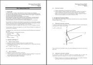

![td-res-4 [Compatibility Mode]](https://img.yumpu.com/45826987/1/184x260/td-res-4-compatibility-mode.jpg?quality=85)