Single-Chip Low Cost Low Power RF-Transceiver (Rev. A)
Single-Chip Low Cost Low Power RF-Transceiver (Rev. A)
Single-Chip Low Cost Low Power RF-Transceiver (Rev. A)

Create successful ePaper yourself
Turn your PDF publications into a flip-book with our unique Google optimized e-Paper software.
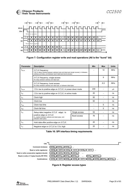
CC2500t spt cht clt sdt hdt nsSCLK:CSn:Write to register:X 0 A6 A5 A4 A3 A2 A1 A0 X D 7 D 6 D 5 D 4 D 3 D 2 D 1 D 0 XSIW W W W W W W WHi-Z S7 S 6 S 5 S4 S 3 S 2 S 1 S0 S7 S6 S5 S4 S3 S2 S1 S0 S7 Hi-ZSORead from register:X 1 A6 A5 A4 A3 A2 A1 A0XSID 7 D 6 D 5 D 4 D 3 D 2 D 1 DSO Hi-Z S7 S 6 S 5 S4 S 3 S 2 S 1 S00R R R R R R R RHi-ZFigure 7: Configuration register write and read operations (A6 is the “burst” bit)Parameter Description Min Max Unitsf SCLKSCLK frequency100 ns delay inserted between address byte and data byte (single access), or betweenaddress and data, and between each data byte (burst access).SCLK frequency, single accessNo delay between address and data byteSCLK frequency, burst accessNo delay between address and data byte, or between data bytes- 10 MHz9 MHz6.5 MHzt sp,pd CSn low to positive edge on SCLK, in power-down mode 200 - µst sp CSn low to positive edge on SCLK, in active mode 20 - nst ch Clock high 50 - nst cl Clock low 50 - nst rise Clock rise time - 5 nst fall Clock fall time - 5 nst sdSetup data (negative SCLK edge) topositive edge on SCLK(t sd applies between address and data bytes, andbetween data bytes)<strong>Single</strong> access 55 - nsBurst access 76 - nst hd Hold data after positive edge on SCLK 20 - nst ns Negative edge on SCLK to CSn high 20 - nsTable 16: SPI interface timing requirementsCSn:Command strobe(s):Read or write register(s):Read or write consecutive registers (burst):Read or write n+1 bytes from/to <strong>RF</strong> FIFO:Combinations:ADDR strobeADDR regADDRADDR strobeDATAADDR strobe ...ADDR reg DATAADDR reg n DATA n DATA n+1 DATA n+2 ...ADDR regADDR reg DATA ...FIFODATA byte 0DATA byte 1DATA byte 2 ... DATA byte n-1DATA byte nDATAADDR strobeADDR regDATA ADDR strobeADDR FIFODATA byte 0DATA byte 1 ...Figure 8: Register access typesPRELIMINARY Data Sheet (<strong>Rev</strong>.1.2) SWRS040A Page 20 of 83


![td-res-4 [Compatibility Mode]](https://img.yumpu.com/45826987/1/184x260/td-res-4-compatibility-mode.jpg?quality=85)