Single-Chip Low Cost Low Power RF-Transceiver (Rev. A)
Single-Chip Low Cost Low Power RF-Transceiver (Rev. A)
Single-Chip Low Cost Low Power RF-Transceiver (Rev. A)

You also want an ePaper? Increase the reach of your titles
YUMPU automatically turns print PDFs into web optimized ePapers that Google loves.
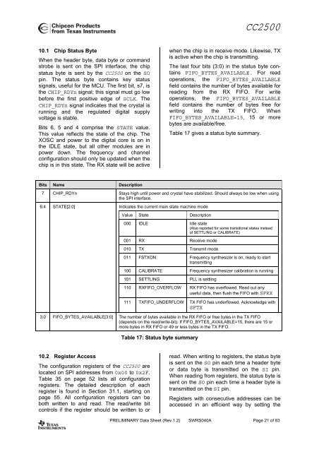
CC250010.1 <strong>Chip</strong> Status ByteWhen the header byte, data byte or commandstrobe is sent on the SPI interface, the chipstatus byte is sent by the CC2500 on the SOpin. The status byte contains key statussignals, useful for the MCU. The first bit, s7, isthe CHIP_RDYn signal; this signal must go lowbefore the first positive edge of SCLK. TheCHIP_RDYn signal indicates that the crystal isrunning and the regulated digital supplyvoltage is stable.Bits 6, 5 and 4 comprise the STATE value.This value reflects the state of the chip. TheXOSC and power to the digital core is on inthe IDLE state, but all other modules are inpower down. The frequency and channelconfiguration should only be updated when thechip is in this state. The RX state will be activewhen the chip is in receive mode. Likewise, TXis active when the chip is transmitting.The last four bits (3:0) in the status byte containsFIFO_BYTES_AVAILABLE. For readoperations, the FIFO_BYTES_AVAILABLEfield contains the number of bytes available forreading from the RX FIFO. For writeoperations, the FIFO_BYTES_AVAILABLEfield contains the number of bytes free forwriting into the TX FIFO. WhenFIFO_BYTES_AVAILABLE=15, 15 or morebytes are available/free.Table 17 gives a status byte summary.Bits Name Description7 CHIP_RDYn Stays high until power and crystal have stabilized. Should always be low when usingthe SPI interface.6:4 STATE[2:0] Indicates the current main state machine modeValue State Description000 IDLE Idle state(Also reported for some transitional states insteadof SETTLING or CALIBRATE)001 RX Receive mode010 TX Transmit mode011 FSTXON Frequency synthesizer is on, ready to starttransmitting100 CALIBRATE Frequency synthesizer calibration is running101 SETTLING PLL is settling110 RXFIFO_OVE<strong>RF</strong>LOW RX FIFO has overflowed. Read out anyuseful data, then flush the FIFO with SFRX111 TXFIFO_UNDE<strong>RF</strong>LOW TX FIFO has underflowed. Acknowledge withSFTX3:0 FIFO_BYTES_AVAILABLE[3:0] The number of bytes available in the RX FIFO or free bytes in the TX FIFO(depends on the read/write-bit). If FIFO_BYTES_AVAILABLE=15, there are 15 ormore bytes in RX FIFO or 49 or less bytes in the TX FIFO.Table 17: Status byte summary10.2 Register AccessThe configuration registers of the CC2500 arelocated on SPI addresses from 0x00 to 0x2F.Table 35 on page 52 lists all configurationregisters. The detailed description of eachregister is found in Section 31.1, starting onpage 55. All configuration registers can beboth written to and read. The read/write bitcontrols if the register should be written to orread. When writing to registers, the status byteis sent on the SO pin each time a header byteor data byte is transmitted on the SI pin.When reading from registers, the status byte issent on the SO pin each time a header byte istransmitted on the SI pin.Registers with consecutive addresses can beaccessed in an efficient way by setting thePRELIMINARY Data Sheet (<strong>Rev</strong>.1.2) SWRS040A Page 21 of 83


![td-res-4 [Compatibility Mode]](https://img.yumpu.com/45826987/1/184x260/td-res-4-compatibility-mode.jpg?quality=85)