Single-Chip Low Cost Low Power RF-Transceiver (Rev. A)
Single-Chip Low Cost Low Power RF-Transceiver (Rev. A)
Single-Chip Low Cost Low Power RF-Transceiver (Rev. A)

You also want an ePaper? Increase the reach of your titles
YUMPU automatically turns print PDFs into web optimized ePapers that Google loves.
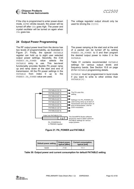
CC2500If the chip is programmed to enter power-downmode, (SPWD strobe issued), the power will beturned off after CSn goes high. The power andcrystal oscillator will be turned on again whenCSn goes low.The voltage regulator output should only beused for driving the CC2500.24 Output <strong>Power</strong> ProgrammingThe <strong>RF</strong> output power level from the device hastwo levels of programmability, as illustrated inFigure 21. Firstly, the special PATABLEregister can hold up to eight user selectedoutput power settings. Secondly, the 3-bitFREND0.PA_POWER value selects thePATABLE entry to use. This two-levelfunctionality provides flexible PA power rampup and ramp down at the start and end oftransmission. All the PA power settings in thePATABLE from index 0 up to theFREND0.PA_POWER value are used.The power ramping at the start and at the endof a packet can be turned off by settingFREND0.PA_POWER to 0 and then programthe desired output power to index 0 in thePATABLE.Table 31 contains recommended PATABLEsettings for various output levels andfrequency bands. See Section 10.6 on page23 for PATABLE programming details.PATABLE must be programmed in burst modeif you want to write to other entries thanPATABLE[0].PATABLE(7)[7:0]PATABLE(6)[7:0]PATABLE(5)[7:0]PATABLE(4)[7:0]PATABLE(3)[7:0]PATABLE(2)[7:0]PATABLE(1)[7:0]PATABLE(0)[7:0]The PA uses thissetting.Settings 0 to PA_POWER areused during ramp-up at start oftransmission and ramp-down atend of transmission, and forOOK modulation.Index into PATABLE(7:0)e.g 6PA_POWER[2:0]in FREND0 registerThe Smart<strong>RF</strong>® Studio softwareshould be used to obtain optimumPATABLE settings for variousoutput powers.Figure 21: PA_POWER and PATABLEDefault power settingOutput power,typical [dBm]Current consumption,typical [mA]0xC6 -11.8 11.1Table 30: Output power and current consumption for default PATABLE settingPRELIMINARY Data Sheet (<strong>Rev</strong>.1.2) SWRS040A Page 42 of 83

![td-res-4 [Compatibility Mode]](https://img.yumpu.com/45826987/1/184x260/td-res-4-compatibility-mode.jpg?quality=85)