Single-Chip Low Cost Low Power RF-Transceiver (Rev. A)
Single-Chip Low Cost Low Power RF-Transceiver (Rev. A)
Single-Chip Low Cost Low Power RF-Transceiver (Rev. A)
You also want an ePaper? Increase the reach of your titles
YUMPU automatically turns print PDFs into web optimized ePapers that Google loves.
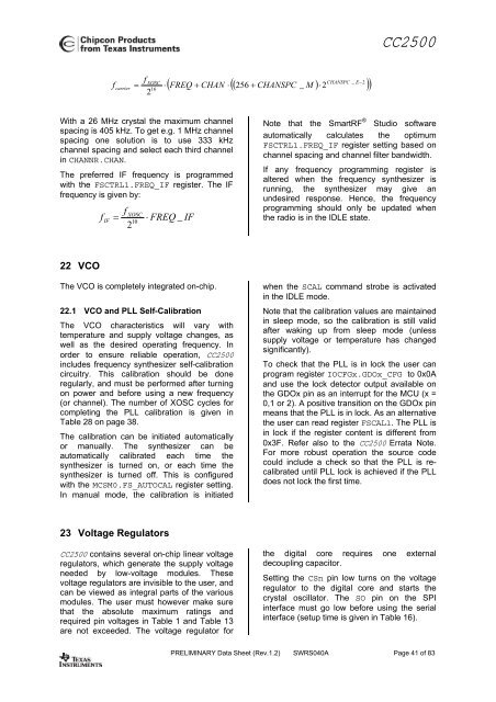
CC2500fcarrier=f2CHANSPC _ E−( FREQ + CHAN ⋅( 256 + CHANSPC _ M ) ⋅2)XOSC⋅216With a 26 MHz crystal the maximum channelspacing is 405 kHz. To get e.g. 1 MHz channelspacing one solution is to use 333 kHzchannel spacing and select each third channelin CHANNR.CHAN.The preferred IF frequency is programmedwith the FSCTRL1.FREQ_IF register. The IFfrequency is given by:fIFfXOSC= ⋅ FREQ _ IF2 10Note that the Smart<strong>RF</strong> ® Studio softwareautomatically calculates the optimumFSCTRL1.FREQ_IF register setting based onchannel spacing and channel filter bandwidth.If any frequency programming register isaltered when the frequency synthesizer isrunning, the synthesizer may give anundesired response. Hence, the frequencyprogramming should only be updated whenthe radio is in the IDLE state.22 VCOThe VCO is completely integrated on-chip.22.1 VCO and PLL Self-CalibrationThe VCO characteristics will vary withtemperature and supply voltage changes, aswell as the desired operating frequency. Inorder to ensure reliable operation, CC2500includes frequency synthesizer self-calibrationcircuitry. This calibration should be doneregularly, and must be performed after turningon power and before using a new frequency(or channel). The number of XOSC cycles forcompleting the PLL calibration is given inTable 28 on page 38.The calibration can be initiated automaticallyor manually. The synthesizer can beautomatically calibrated each time thesynthesizer is turned on, or each time thesynthesizer is turned off. This is configuredwith the MCSM0.FS_AUTOCAL register setting.In manual mode, the calibration is initiatedwhen the SCAL command strobe is activatedin the IDLE mode.Note that the calibration values are maintainedin sleep mode, so the calibration is still validafter waking up from sleep mode (unlesssupply voltage or temperature has changedsignificantly).To check that the PLL is in lock the user canprogram register IOCFGx.GDOx_CFG to 0x0Aand use the lock detector output available onthe GDOx pin as an interrupt for the MCU (x =0,1 or 2). A positive transition on the GDOx pinmeans that the PLL is in lock. As an alternativethe user can read register FSCAL1. The PLL isin lock if the register content is different from0x3F. Refer also to the CC2500 Errata Note.For more robust operation the source codecould include a check so that the PLL is recalibrateduntil PLL lock is achieved if the PLLdoes not lock the first time.23 Voltage RegulatorsCC2500 contains several on-chip linear voltageregulators, which generate the supply voltageneeded by low-voltage modules. Thesevoltage regulators are invisible to the user, andcan be viewed as integral parts of the variousmodules. The user must however make surethat the absolute maximum ratings andrequired pin voltages in Table 1 and Table 13are not exceeded. The voltage regulator forthe digital core requires one externaldecoupling capacitor.Setting the CSn pin low turns on the voltageregulator to the digital core and starts thecrystal oscillator. The SO pin on the SPIinterface must go low before using the serialinterface (setup time is given in Table 16).PRELIMINARY Data Sheet (<strong>Rev</strong>.1.2) SWRS040A Page 41 of 83





![td-res-4 [Compatibility Mode]](https://img.yumpu.com/45826987/1/184x260/td-res-4-compatibility-mode.jpg?quality=85)
