Single-Chip Low Cost Low Power RF-Transceiver (Rev. A)
Single-Chip Low Cost Low Power RF-Transceiver (Rev. A)
Single-Chip Low Cost Low Power RF-Transceiver (Rev. A)

You also want an ePaper? Increase the reach of your titles
YUMPU automatically turns print PDFs into web optimized ePapers that Google loves.
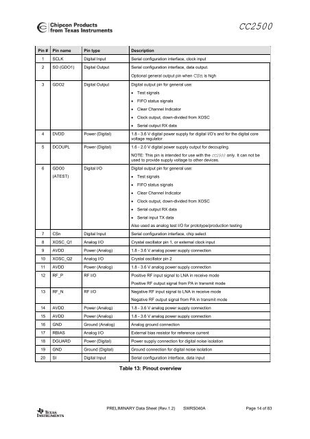
CC2500Pin # Pin name Pin type Description1 SCLK Digital Input Serial configuration interface, clock input2 SO (GDO1) Digital Output Serial configuration interface, data output.Optional general output pin when CSn is high3 GDO2 Digital Output Digital output pin for general use:• Test signals• FIFO status signals• Clear Channel Indicator• Clock output, down-divided from XOSC• Serial output RX data4 DVDD <strong>Power</strong> (Digital) 1.8 - 3.6 V digital power supply for digital I/O’s and for the digital corevoltage regulator5 DCOUPL <strong>Power</strong> (Digital) 1.6 - 2.0 V digital power supply output for decoupling.NOTE: This pin is intended for use with the CC2500 only. It can not beused to provide supply voltage to other devices.6 GDO0(ATEST)Digital I/ODigital output pin for general use:• Test signals• FIFO status signals• Clear Channel Indicator• Clock output, down-divided from XOSC• Serial output RX data• Serial input TX dataAlso used as analog test I/O for prototype/production testing7 CSn Digital Input Serial configuration interface, chip select8 XOSC_Q1 Analog I/O Crystal oscillator pin 1, or external clock input9 AVDD <strong>Power</strong> (Analog) 1.8 - 3.6 V analog power supply connection10 XOSC_Q2 Analog I/O Crystal oscillator pin 211 AVDD <strong>Power</strong> (Analog) 1.8 - 3.6 V analog power supply connection12 <strong>RF</strong>_P <strong>RF</strong> I/O Positive <strong>RF</strong> input signal to LNA in receive modePositive <strong>RF</strong> output signal from PA in transmit mode13 <strong>RF</strong>_N <strong>RF</strong> I/O Negative <strong>RF</strong> input signal to LNA in receive modeNegative <strong>RF</strong> output signal from PA in transmit mode14 AVDD <strong>Power</strong> (Analog) 1.8 - 3.6 V analog power supply connection15 AVDD <strong>Power</strong> (Analog) 1.8 - 3.6 V analog power supply connection16 GND Ground (Analog) Analog ground connection17 RBIAS Analog I/O External bias resistor for reference current18 DGUARD <strong>Power</strong> (Digital) <strong>Power</strong> supply connection for digital noise isolation19 GND Ground (Digital) Ground connection for digital noise isolation20 SI Digital Input Serial configuration interface, data inputTable 13: Pinout overviewPRELIMINARY Data Sheet (<strong>Rev</strong>.1.2) SWRS040A Page 14 of 83

![td-res-4 [Compatibility Mode]](https://img.yumpu.com/45826987/1/184x260/td-res-4-compatibility-mode.jpg?quality=85)