Single-Chip Low Cost Low Power RF-Transceiver (Rev. A)
Single-Chip Low Cost Low Power RF-Transceiver (Rev. A)
Single-Chip Low Cost Low Power RF-Transceiver (Rev. A)

You also want an ePaper? Increase the reach of your titles
YUMPU automatically turns print PDFs into web optimized ePapers that Google loves.
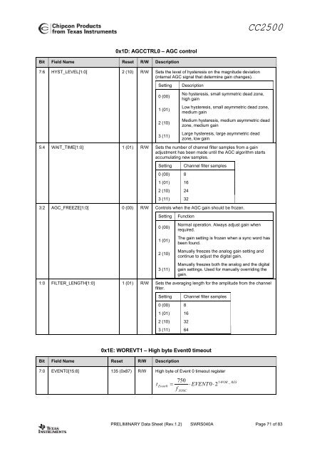
CC25000x1D: AGCCTRL0 – AGC controlBit Field Name Reset R/W Description7:6 HYST_LEVEL[1:0] 2 (10) R/W Sets the level of hysteresis on the magnitude deviation(internal AGC signal that determine gain changes).Setting0 (00)1 (01)2 (10)3 (11)DescriptionNo hysteresis, small symmetric dead zone,high gain<strong>Low</strong> hysteresis, small asymmetric dead zone,medium gainMedium hysteresis, medium asymmetric deadzone, medium gainLarge hysteresis, large asymmetric deadzone, low gain5:4 WAIT_TIME[1:0] 1 (01) R/W Sets the number of channel filter samples from a gainadjustment has been made until the AGC algorithm startsaccumulating new samples.Setting0 (00) 81 (01) 162 (10) 243 (11) 32Channel filter samples3:2 AGC_FREEZE[1:0] 0 (00) R/W Controls when the AGC gain should be frozen.Setting0 (00)1 (01)2 (10)3 (11)FunctionNormal operation. Always adjust gain whenrequired.The gain setting is frozen when a sync word hasbeen found.Manually freezes the analog gain setting andcontinue to adjust the digital gain.Manually freezes both the analog and the digitalgain settings. Used for manually overriding thegain.1:0 FILTER_LENGTH[1:0] 1 (01) R/W Sets the averaging length for the amplitude from the channelfilter.Setting0 (00) 81 (01) 162 (10) 323 (11) 64Channel filter samples0x1E: WOREVT1 – High byte Event0 timeoutBit Field Name Reset R/W Description7:0 EVENT0[15:8] 135 (0x87) R/W High byte of Event 0 timeout registert750 ⋅5 WOR _ RESEvent0 = ⋅ EVENT0⋅2fXOSCPRELIMINARY Data Sheet (<strong>Rev</strong>.1.2) SWRS040A Page 71 of 83

![td-res-4 [Compatibility Mode]](https://img.yumpu.com/45826987/1/184x260/td-res-4-compatibility-mode.jpg?quality=85)