Single-Chip Low Cost Low Power RF-Transceiver (Rev. A)
Single-Chip Low Cost Low Power RF-Transceiver (Rev. A)
Single-Chip Low Cost Low Power RF-Transceiver (Rev. A)
Create successful ePaper yourself
Turn your PDF publications into a flip-book with our unique Google optimized e-Paper software.
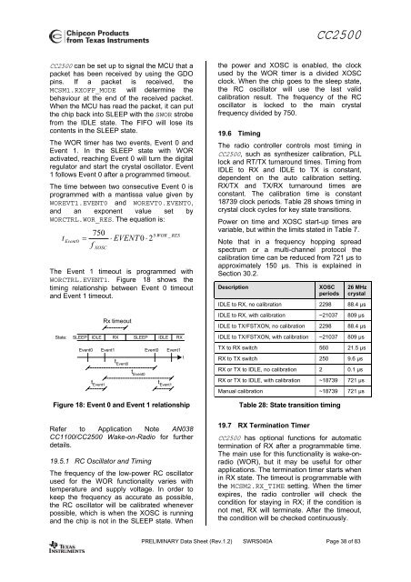
CC2500CC2500 can be set up to signal the MCU that apacket has been received by using the GDOpins. If a packet is received, theMCSM1.RXOFF_MODE will determine thebehaviour at the end of the received packet.When the MCU has read the packet, it can putthe chip back into SLEEP with the SWOR strobefrom the IDLE state. The FIFO will lose itscontents in the SLEEP state.The WOR timer has two events, Event 0 andEvent 1. In the SLEEP state with WORactivated, reaching Event 0 will turn the digitalregulator and start the crystal oscillator. Event1 follows Event 0 after a programmed timeout.The time between two consecutive Event 0 isprogrammed with a mantissa value given byWOREVT1.EVENT0 and WOREVT0.EVENT0,and an exponent value set byWORCTRL.WOR_RES. The equation is:t750 ⋅5 WOR _ RESEvent0 = ⋅ EVENT 0 ⋅ 2fXOSCThe Event 1 timeout is programmed withWORCTRL.EVENT1. Figure 18 shows thetiming relationship between Event 0 timeoutand Event 1 timeout.State:Event0 Event1 Event0t Event1Rx timeoutSLEEP IDLE RX SLEEP IDLE RXt Event0t Event0t Event1Event1Figure 18: Event 0 and Event 1 relationshiptthe power and XOSC is enabled, the clockused by the WOR timer is a divided XOSCclock. When the chip goes to the sleep state,the RC oscillator will use the last validcalibration result. The frequency of the RCoscillator is locked to the main crystalfrequency divided by 750.19.6 TimingThe radio controller controls most timing inCC2500, such as synthesizer calibration, PLLlock and RT/TX turnaround times. Timing fromIDLE to RX and IDLE to TX is constant,dependent on the auto calibration setting.RX/TX and TX/RX turnaround times areconstant. The calibration time is constant18739 clock periods. Table 28 shows timing incrystal clock cycles for key state transitions.<strong>Power</strong> on time and XOSC start-up times arevariable, but within the limits stated in Table 7.Note that in a frequency hopping spreadspectrum or a multi-channel protocol thecalibration time can be reduced from 721 µs toapproximately 150 µs. This is explained inSection 30.2.DescriptionXOSCperiods26 MHzcrystalIDLE to RX, no calibration 2298 88.4 µsIDLE to RX, with calibration ~21037 809 µsIDLE to TX/FSTXON, no calibration 2298 88.4 µsIDLE to TX/FSTXON, with calibration ~21037 809 µsTX to RX switch 560 21.5 µsRX to TX switch 250 9.6 µsRX or TX to IDLE, no calibration 2 0.1 µsRX or TX to IDLE, with calibration ~18739 721 µsManual calibration ~18739 721 µsTable 28: State transition timingRefer to Application Note AN038CC1100/CC2500 Wake-on-Radio for furtherdetails.19.5.1 RC Oscillator and TimingThe frequency of the low-power RC oscillatorused for the WOR functionality varies withtemperature and supply voltage. In order tokeep the frequency as accurate as possible,the RC oscillator will be calibrated wheneverpossible, which is when the XOSC is runningand the chip is not in the SLEEP state. When19.7 RX Termination TimerCC2500 has optional functions for automatictermination of RX after a programmable time.The main use for this functionality is wake-onradio(WOR), but it may be useful for otherapplications. The termination timer starts whenin RX state. The timeout is programmable withthe MCSM2.RX_TIME setting. When the timerexpires, the radio controller will check thecondition for staying in RX; if the condition isnot met, RX will terminate. After the timeout,the condition will be checked continuously.PRELIMINARY Data Sheet (<strong>Rev</strong>.1.2) SWRS040A Page 38 of 83



![td-res-4 [Compatibility Mode]](https://img.yumpu.com/45826987/1/184x260/td-res-4-compatibility-mode.jpg?quality=85)
