ABCs of ADCs - Analog-to-Digital Converter Basics (PDF)
ABCs of ADCs - Analog-to-Digital Converter Basics (PDF)
ABCs of ADCs - Analog-to-Digital Converter Basics (PDF)

Create successful ePaper yourself
Turn your PDF publications into a flip-book with our unique Google optimized e-Paper software.
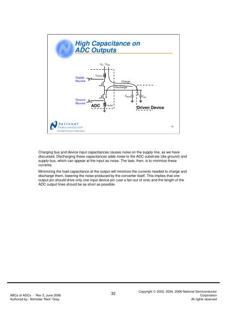
High Capacitance onADC OutputsV D / V DRSupplyBounceL BONDChargeDischargeGroundBounceADCL BONDC BUSC INDriven Device32Charging bus and device input capacitances causes noise on the supply line, as we havediscussed. Discharging these capacitances adds noise <strong>to</strong> the ADC substrate (die ground) andsupply bus, which can appear at the input as noise. The task, then, is <strong>to</strong> minimize thesecurrents.Minimizing the load capacitance at the output will minimize the currents needed <strong>to</strong> charge anddischarge them, lowering the noise produced by the converter itself. This implies that oneoutput pin should drive only one input device pin (use a fan-out <strong>of</strong> one) and the length <strong>of</strong> theADC output lines should be as short as possible.<strong>ABCs</strong> <strong>of</strong> <strong>ADCs</strong> - Rev 3, June 2006Authored by: Nicholas “Nick” Gray32Copyright © 2003, 2004, 2006 National Semiconduc<strong>to</strong>rCorporationAll rights reserved