ABCs of ADCs - Analog-to-Digital Converter Basics (PDF)
ABCs of ADCs - Analog-to-Digital Converter Basics (PDF)
ABCs of ADCs - Analog-to-Digital Converter Basics (PDF)

You also want an ePaper? Increase the reach of your titles
YUMPU automatically turns print PDFs into web optimized ePapers that Google loves.
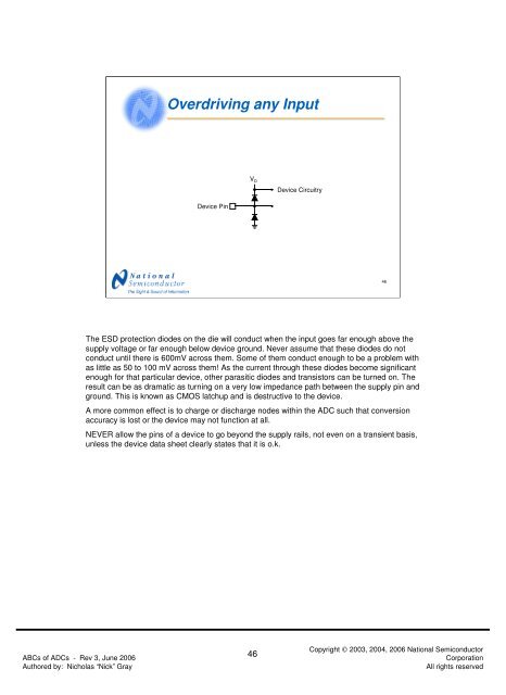
Overdriving any InputV DDevice CircuitryDevice Pin46The ESD protection diodes on the die will conduct when the input goes far enough above thesupply voltage or far enough below device ground. Never assume that these diodes do notconduct until there is 600mV across them. Some <strong>of</strong> them conduct enough <strong>to</strong> be a problem withas little as 50 <strong>to</strong> 100 mV across them! As the current through these diodes become significantenough for that particular device, other parasitic diodes and transis<strong>to</strong>rs can be turned on. Theresult can be as dramatic as turning on a very low impedance path between the supply pin andground. This is known as CMOS latchup and is destructive <strong>to</strong> the device.A more common effect is <strong>to</strong> charge or discharge nodes within the ADC such that conversionaccuracy is lost or the device may not function at all.NEVER allow the pins <strong>of</strong> a device <strong>to</strong> go beyond the supply rails, not even on a transient basis,unless the device data sheet clearly states that it is o.k.<strong>ABCs</strong> <strong>of</strong> <strong>ADCs</strong> - Rev 3, June 2006Authored by: Nicholas “Nick” Gray46Copyright © 2003, 2004, 2006 National Semiconduc<strong>to</strong>rCorporationAll rights reserved