ABCs of ADCs - Analog-to-Digital Converter Basics (PDF)
ABCs of ADCs - Analog-to-Digital Converter Basics (PDF)
ABCs of ADCs - Analog-to-Digital Converter Basics (PDF)

You also want an ePaper? Increase the reach of your titles
YUMPU automatically turns print PDFs into web optimized ePapers that Google loves.
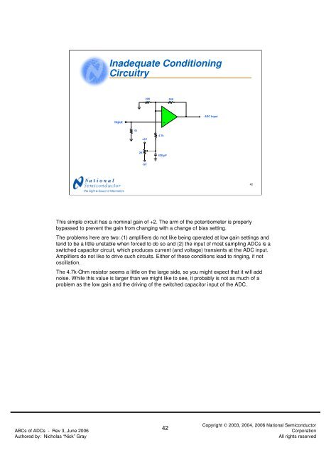
Inadequate ConditioningCircuitry220 220-Input+ADC Input51+5V4.7k2K430 pF-5V42This simple circuit has a nominal gain <strong>of</strong> +2. The arm <strong>of</strong> the potentiometer is properlybypassed <strong>to</strong> prevent the gain from changing with a change <strong>of</strong> bias setting.The problems here are two: (1) amplifiers do not like being operated at low gain settings andtend <strong>to</strong> be a little unstable when forced <strong>to</strong> do so and (2) the input <strong>of</strong> most sampling <strong>ADCs</strong> is aswitched capaci<strong>to</strong>r circuit, which produces current (and voltage) transients at the ADC input.Amplifiers do not like <strong>to</strong> drive such circuits. Either <strong>of</strong> these conditions lead <strong>to</strong> ringing, if no<strong>to</strong>scillation.The 4.7k-Ohm resis<strong>to</strong>r seems a little on the large side, so you might expect that it will addnoise. While this value is larger than we might like <strong>to</strong> see, it probably is not as much <strong>of</strong> aproblem as the low gain and the driving <strong>of</strong> the switched capaci<strong>to</strong>r input <strong>of</strong> the ADC.<strong>ABCs</strong> <strong>of</strong> <strong>ADCs</strong> - Rev 3, June 2006Authored by: Nicholas “Nick” Gray42Copyright © 2003, 2004, 2006 National Semiconduc<strong>to</strong>rCorporationAll rights reserved