
Create successful ePaper yourself
Turn your PDF publications into a flip-book with our unique Google optimized e-Paper software.
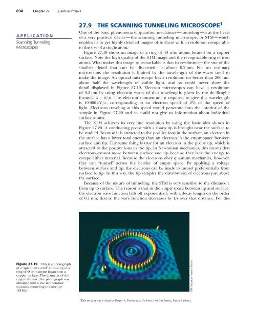
894 Chapter 27 <strong>Quantum</strong> <strong>Physics</strong>APPLICATIONScanning TunnelingMicroscopes27.9 THE SCANNING TUNNELING MICROSCOPE 1One of the basic phenomena of quantum mechanics—tunneling—is at the heartof a very practical device—the scanning tunneling microscope, or STM—whichenables us to get highly detailed images of surfaces with a resolution comparableto the size of a single atom.Figure 27.19 shows an image of a ring of 48 iron atoms located on a coppersurface. Note the high quality of the STM image and the recognizable ring of ironatoms. What makes this image so remarkable is that its resolution—the size of thesmallest detail that can be discerned—is about 0.2 nm. For an ordinarymicroscope, the resolution is limited by the wavelength of the waves used tomake the image. An optical microscope has a resolution no better than 200 nm,about half the wavelength of visible light, and so could never show thedetail displayed in Figure 27.19. Electron microscopes can have a resolutionof 0.2 nm by using electron waves of that wavelength, given by the de Broglieformula h/p. The electron momentum p required to give this wavelengthis 10 000 eV/c, corresponding to an electron speed of 2% of the speed oflight. Electrons traveling at this speed would penetrate into the interior of thesample in Figure 27.20 and so could not give us information about individualsurface atoms.The STM achieves its very fine resolution by using the basic idea shown inFigure 27.20. A conducting probe with a sharp tip is brought near the surface tobe studied. Because it is attracted to the positive ions in the surface, an electron inthe surface has a lower total energy than an electron in the empty space betweensurface and tip. The same thing is true for an electron in the probe tip, which isattracted to the positive ions in the tip. In Newtonian mechanics, this means thatelectrons cannot move between surface and tip because they lack the energy toescape either material. Because the electrons obey quantum mechanics, however,they can “tunnel” across the barrier of empty space. By applying a voltagebetween surface and tip, the electrons can be made to tunnel preferentially fromsurface to tip. In this way, the tip samples the distribution of electrons just abovethe surface.Because of the nature of tunneling, the STM is very sensitive to the distance zfrom tip to surface. The reason is that in the empty space between tip and surface,the electron wave function falls off exponentially with a decay length on the orderof 0.1 nm; that is, the wave function decreases by 1/e over that distance. For dis-Figure 27.19 This is a photographof a “quantum corral” consisting of aring of 48 iron atoms located on acopper surface. The diameter of thering is 143 nm. The photograph wasobtained with a low-temperaturescanning tunneling microscope(STM).IBM Corporation Research Division1 This section was written by Roger A. Freedman, University of California, Santa Barbara.