
You also want an ePaper? Increase the reach of your titles
YUMPU automatically turns print PDFs into web optimized ePapers that Google loves.
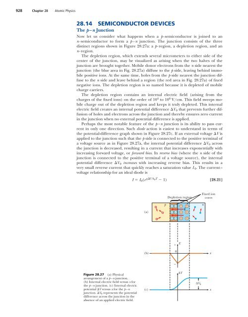
928 Chapter 28 Atomic <strong>Physics</strong>28.14 SEMICONDUCTOR DEVICESThe p–n JunctionNow let us consider what happens when a p -semiconductor is joined to ann -semiconductor to form a p–n junction. The junction consists of the threedistinct regions shown in Figure 28.27a: a p -region, a depletion region, and ann -region.The depletion region, which extends several micrometers to either side of thecenter of the junction, may be visualized as arising when the two halves of thejunction are brought together. Mobile donor electrons from the n side nearest thejunction (the blue area in Fig. 28.27a) diffuse to the p side, leaving behind immobilepositive ions. At the same time, holes from the p side nearest the junction diffuseto the n side and leave behind a region (the red area in Fig. 28.27a) of fixednegative ions. The depletion region is so named because it is depleted of mobilecharge carriers.The depletion region contains an internal electric field (arising from thecharges of the fixed ions) on the order of 10 4 to 10 6 V/cm. This field sweeps mobilecharge out of the depletion region and keeps it truly depleted. This internalelectric field creates an internal potential difference V 0 that prevents further diffusionof holes and electrons across the junction and thereby ensures zero currentin the junction when no external potential difference is applied.Perhaps the most notable feature of the p–n junction is its ability to pass currentin only one direction. Such diode action is easiest to understand in terms ofthe potential-difference graph shown in Figure 28.27c. If an external voltage V isapplied to the junction such that the p side is connected to the positive terminal ofa voltage source as in Figure 28.27a, the internal potential difference V 0 acrossthe junction is decreased, resulting in a current that increases exponentially withincreasing forward voltage, or forward bias. In reverse bias (where the n side of thejunction is connected to the positive terminal of a voltage source), the internalpotential difference V 0 increases with increasing reverse bias. This results in avery small reverse current that quickly reaches a saturation value I 0 . The current–voltage relationship for an ideal diode isI I 0 (e q V/k BT 1)[28.21]Depletion regionFixed ioncores(a)p––––+ +E+ +n––+ ++E(b)0x–Figure 28.27 (a) Physicalarrangement of a p–n junction.(b) Internal electric field versus x forthe p–n junction. (c) Internal electricpotential V versus x for the p–njunction. V 0 represents the potentialdifference across the junction in theabsence of an applied electric field.(c)∆V∆V 0x