

March - April 2010 - Chip Scale Review
March - April 2010 - Chip Scale Review
March - April 2010 - Chip Scale Review

Create successful ePaper yourself
Turn your PDF publications into a flip-book with our unique Google optimized e-Paper software.
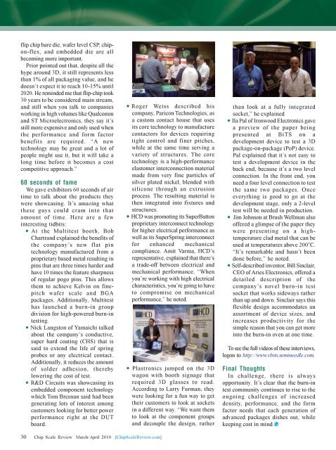
flip chip bare die, wafer level CSP, chipon-flex,and embedded die are allbecoming more important.Prior pointed out that, despite all thehype around 3D, it still represents lessthan 1% of all packaging value, and hedoesn’t expect it to reach 10-15% until2020. He reminded me that flip-chip took30 years to be considered main stream,and still when you talk to companiesworking in high volumes like Qualcommand ST Microelectronics, they say it’sstill more expensive and only used whenthe performance and form factorbenefits are required. “A newtechnology may be great and a lot ofpeople might use it, but it will take along time before it becomes a costcompetitive approach.”60 seconds of fameWe gave exhibitors 60 seconds of airtime to talk about the products theywere showcasing. It’s amazing whatthese guys could cram into thatamount of time. Here are a fewinteresting tidbits:● At the Multitest booth, BobChartrand explained the benefits ofthe company’s new flat pintechnology manufactured from aproprietary based metal resulting inpins that are three times harder andhave 10 times the feature sharpnessof regular pogo pins. This allowsthem to achieve Kelvin on finepitchwafer scale and BGApackages. Additionally, Multitesthas launched a burn-in groupdivision for high-powered burn-intesting.● Nick Langston of Yamaichi talkedabout the company’s conductive,super hard coating (CHS) that issaid to extend the life of springprobes or any electrical contact.Additionally, it reduces the amountof solder adhesion, therebylowering the cost of test.● R&D Circuits was showcasing itsembedded component technologywhich Tom Bresnan said had beengenerating lots of interest amongcustomers looking for better powerperformance right at the DUTboard.●Roger Weiss described hiscompany, Paricon Technologies, asa custom contact house that usesits core technology to manufacturecontactors for devices requiringtight control and finer pitches,while at the same time serving avariety of structures. The coretechnology is a high-performanceelastomer interconnection materialmade from very fine particles ofsilver plated nickel, blended withsilicone through an extrusionprocess. The resulting material isthen integrated into fixtures andstructures.● HCD was promoting its SuperButtonproprietary interconnect technologyfor higher electrical performance aswell as its SuperSpring interconnectfor enhanced mechanicalcompliance. Amit Varma, HCD’srepresentative, explained that there’sa trade-off between electrical andmechanical performance. “Whenyou’re working with high electricalcharacteristics, you’re going to haveto compromise on mechanicalperformance,” he noted.● Plastronics jumped on the 3Dwagon with booth signage thatrequired 3D glasses to read.According to Larry Furman, theywere looking for a fun way to gettheir customers to look at socketsin a different way. “We want themto look at the component groupsand decouple the design, ratherthan look at a fully integratedsocket,” he explained● Ila Pal of Ironwood Electronics gavea preview of the paper beingpresented at BiTS on adevelopment device to test a 3Dpackage-on-package (PoP) device.Pal explained that it’s not easy totest a development device in theback end, because it’s a two levelconnection. In the front end, youneed a four level connection to testthe same two packages. Onceeverything is good to go at thedevelopment stage, only a 2-leveltest will be needed in production.● Jim Johnson at Brush Wellman alsooffered a glimpse of the paper theywere presenting on a hightemperatureclad metal that can beused at temperatures above 200 o C.“It’s remarkable and hasn’t beendone before,” he noted.● Self-described inventor, Bill Sinclair,CEO of Aries Electronics, offered adetailed description of thecompany’s novel burn-in testsocket that works sideways ratherthan up and down. Sinclair says thisflexible design accommodates anassortment of device sizes, andincreases productivity for thesimple reason that you can get moreinto the burn-in oven at one time.To see the full videos of these interviews,logon to http://www.vbits.semineedle.com.Final ThoughtsIn challenge, there is alwaysopportunity. It’s clear that the burn-intest community continues to rise to theongoing challenges of increaseddensity, performance, and the formfactor needs that each generation ofadvanced packages dishes out, whilekeeping cost in mind.30<strong>Chip</strong> <strong>Scale</strong> <strong>Review</strong>. <strong>March</strong>/<strong>April</strong> <strong>2010</strong> . [<strong>Chip</strong><strong>Scale</strong><strong>Review</strong>.com]


