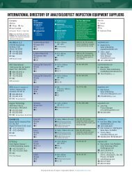
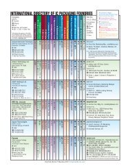
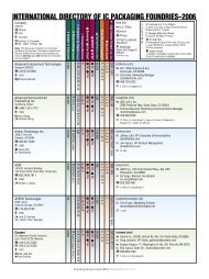
INTERNATIONAL DIRECTORY OF WAFER-BUMPING SERVICE PROVIDERSNotes: This list was compiled from data supplied by the respective providers and is not all-inclusive as to company or service offered. Advertisers in this issue are indicatedby boldface listings. CM=Consult Manufacturer.CompanyAddressCity, State, ZipCountryPhoneFaxFounding YearNumber of EmployeesMaximum Wafer Size (mm)Bump Pitches (µm)Bumping ServicesEquipmentA=Aligners, B=Stencil Printers, C=SteppersBumping TechnologiesJ=Jetting, P=Plating, BP=Ball/loading placement,S=Sputtered, SP=Stencil printing,CP=Copper pillar, O=OtherBump AlloysSAC=SnAgCu, Au=Gold, Eu=Eutectic,LF=Pb-free, HL=High lead, LA=Low alphaWebSiteContactAdditional OfficesInternational Micro Industries (IMI )1951 Old Cuthbert Rd. Bldg 404Cherry Hill, NJ 08034Tel: 856-616-0226Fax: 856-616-02261971 ( Founded )21300CMBumping and WLP utilizing electrodeposition process and specializing inhigh aspect ratio, fine pitch and pillarbump technologyAlignersP, S, CP, OSAC ( SnAgCu )Au, E, LF, HLwww.imi-corp.comMinami Co., Ltd.EMS Tsukuba Factory 38-325-Chome, Minami-Cho Fuchu-Shi,Tokyo 183-0026, JapanTel: +81.42.368.831119803030080µm (45µm diameter)Ball placement, reflow, washing, inspection,quick delivery, low cost, high qualityCMSP T P, SP, BPSolder paste and balls, SnAgCuwww.ho-minami.co.jpNEPES, Pte Ltd12 Ang Mo Kio Street 65Singapore 569060Tel: +65-6412-8181CM30050 – 150Turnkey solution for Bumping, Testingand Wafer Level PackagingCMP, S, CPLF, HL, Eu, Cuwww.nepes.com.sgPac Tech GmbHDivision of Nagase & Co., LtdAm Schlangenhorst 7-9 & 15-1714641 Nauen, GermanyTel: +49.3321.4495.100Fax:+49.3321.4495.110 .1995150300UBM 40µm, bump pitch solder 80µmWafer bumping for Ni/Au UBM, Ni/Pd/Auand thick Au for wire bonding; waferlevel solder bumping, BCB repassivation,wafer level redistribution, wafer thinning,wafer dicing, chip singulation, tape & reelASP T SP, BP, electroless UBM, JUBM: NiAu, NiPdAu; Solder:SnAgCu, SnPb, AuSnwww.pactech.dePac Tech USA Inc.,328 Martin Ave.,Santa Clara, CA 95050Tel: 408.588.1925Pac Tech Asia Sdn Bhd.,Bayan Lepas IndustrialZone, 11900 Bayan Lepas,Penang, MalaysiaSiliconware Precision Industries Co.Tantzu, Taichung, 427 TaiwanTel: +886.4.253415251984~14,800300180CMA, B, CP, SP, BP, sputtered UBMSn63/Pb37, Sn5/Pb95, SnAgCu,SnAg, SnCu, Au bumpwww.spil.com.twSiliconware USA Inc.,San Jose, CA 95110Tel: 888.215.8632STATS <strong>Chip</strong>PAC Ltd.Singapore 569059Tel: +65.6824.7777199414,873300CMPrinted, plated and ball drop bump,redistribution, flip chip interconnectand WLCSPA, B, CP, SP, BP, sputtered UBMEu, ultra low alpha HL, LFwww.statschippac.comSTATS <strong>Chip</strong>PAC Inc.,Fremont, CA 94538Tel: 510.979.8000All Companies listed have in-house wafer bumping capabilitiesListing does not include capability for Gold Wire Ball Bumping.The <strong>2010</strong> International Directory of Wafer Bumping Service Providers is compiled by AZ Tech Direct LLC.To update listings in the directory for next year’s publication, please contact the author at surveys@aztechdirect.com before January 31, 2011.36<strong>Chip</strong> <strong>Scale</strong> <strong>Review</strong>. <strong>March</strong>/<strong>April</strong> <strong>2010</strong> . [<strong>Chip</strong><strong>Scale</strong><strong>Review</strong>.com]
WHAT'S NEW!Nanoscale MEMS Made Inside aCMOS WaferA new technology to constructnanoscale MEMS within the structureof the actual CMOS wafer itself usingstandard, high volume CMOS lines, hasbeen announced by BoalabMicrosystems of Barcelona, Spain. Thetechnology uses the existing metallayers in a CMOS wafer to form theMEMS structure using standard masktechniques. “We have solved thechallenge of building MEMS in acompletely different way,” explainedDave Doyle, Baolab’s CEO.Baolab has successfully createdMEMS devices using standard 0.18μm,8” CMOS wafers with four or moremetal layers, and has achievedminimum feature sizes down to 200nanometres. The prototype stage hasalready proven the NanoEMStechnology and evaluation sampleswill be available later this year. Theseare aimed at handset designers andmanufacturers, and Power Amplifierand RF Front End Module markets.[www.baolab.com]Gantry Robots Get More CapacityDENSO, headquartered in Kariya,Japan, has announced that it hasincreased the payload capacity of itsXR-Series four-axis, compact gantryrobots from 3 kg to 5 kg. The new 5kgcapacity, which represents an increaseof over 60 percent, allows the robots tohandle a significantly wider range ofapplications. The XR-Series robotsfeature a ceiling mounted, SCARA robotcombined with a long-stroke Cartesianrobot. They can operate in manyapplications without the need of aconveyor.The robots havea reach of 200mm to300mm, an x-axisstroke of 850mm to1,660mm, a cycletime of 0.53seconds, andrepeatability of± 0.015mm. Typicalapplicationsinclude assembly, dispensing, materialhandling, and parts feeding. DENSORobotics offer robots, controllers andsoftware covering a wide range ofapplications. [www.densorobotics.com]Need a Class 100 Oven?The No. 836 is a 750 O F, electricallyheated,Class 100 cleanroom oven fromGrieve, Round Lake, IL, USA, and canbe used to bake various coatings ontoproducts at a customer’s facility.Workspace dimensions of this ovenmeasure 36” wide x 36” deep x 39” high.Incoloy sheathed tubular heatingelements provide 30KW of heating anda maximum temperature of 750 O F. A1000CFM, 1.5HP recirculating blowermaintains horizontal airflow across theload. The oven has 6” insulated walls,a 2B finish stainless steel interior, andan aluminized exterior.Additional equipment on this Grieveoven include a 30” x 24” x 6” thickstainless steel high temperature HEPArecirculating air filter, digitalprogramming temperature controller,manual reset excess temperaturecontroller with separate contactors,recirculating blower airflow safetyswitch, and a 10” diameter circular chartrecorder.[www.grievecorp.com]New Test Socket Claims 500,000InsertionsIronwood Electronics of Burnsville,MN, USA, has recently introduced thenew high performance socket for the602PGA-SS-PGA27/602A-01. Thecontactor is a spring pin (pogo) with27 grams actuation force per ball andcycle life of 500,000 insertions. Theself-inductance of the contactor is1.1nH with 50Ω matched impedance.The current capacity of each contactoris 5 amps. Socket temperature range is-55°C to +150°C. Kyocera’sPB602AUE63-1 and other PGA ICs thatare 35x35mm body size, 1.27mm pitch,and 27x27 pin array can be tested. TheSocket is constructed of aluminumwhich provides heat sinking up toseveral watts and custom heat sinkscan easily be designed for higherpower dissipation. This socket can beused for functional test and extremethermal cycling test with the moststringent requirements.[www.ironwoodelectronics.com]Bond Tester Has More FeaturesThe Condor EZ, a new bond testerfrom XYZTEC, Gilroy, CA, USA, offersa singleplatform withmultiple testcapabilities.In additionto standardbond testingapplicationssuch as wire<strong>Chip</strong> <strong>Scale</strong> <strong>Review</strong>. <strong>March</strong>/<strong>April</strong> <strong>2010</strong> . [<strong>Chip</strong><strong>Scale</strong><strong>Review</strong>.com] 37


