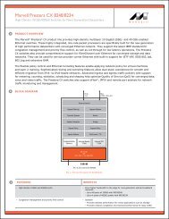
Marvell PXA27x Processor Family
PXA27x Design Guide - Marvell
PXA27x Design Guide - Marvell

You also want an ePaper? Increase the reach of your titles
YUMPU automatically turns print PDFs into web optimized ePapers that Google loves.
<strong>PXA27x</strong> <strong>Processor</strong> <strong>Family</strong><br />
Design Guide<br />
18.3 Block Diagram......................................................................................................................... 189<br />
18.4 Layout Notes ........................................................................................................................... 191<br />
Section 19.Universal Serial Bus Host Interface ............................................................. 193<br />
19.1 Overview ................................................................................................................................. 193<br />
19.2 Signals .................................................................................................................................... 193<br />
19.3 Block Diagrams ....................................................................................................................... 193<br />
19.3.1 Block Diagram for USB Host Differential Connection (Port 1 or Port 2) ....................................... 193<br />
19.3.2 Block Diagrams for USB Host Port 2 (Differential or Single-Ended) ............................................ 194<br />
19.3.3 Block Diagram for USB Host Single-Ended Connection (Port 3) ................................................. 195<br />
19.4 Layout Notes ........................................................................................................................... 196<br />
Section 20.Real Time Clock Interface ............................................................................. 199<br />
20.1 Overview ................................................................................................................................. 199<br />
20.2 Signals .................................................................................................................................... 199<br />
20.3 Block Diagram......................................................................................................................... 199<br />
20.4 Layout Notes ........................................................................................................................... 200<br />
Section 21.OS Timer Interface ......................................................................................... 201<br />
21.1 Overview ................................................................................................................................. 201<br />
21.2 Signals .................................................................................................................................... 201<br />
21.3 Block Diagram......................................................................................................................... 202<br />
21.3.1 Channel Access/Control Block ..................................................................................................... 202<br />
21.3.2 PXA25x Compatibility Channels 0-3 Block................................................................................... 202<br />
21.3.3 Channels 4 - 11 Blocks................................................................................................................. 202<br />
21.3.4 Output Control .............................................................................................................................. 203<br />
21.4 Layout Notes ........................................................................................................................... 203<br />
Section 22.Pulse-Width Modulator Interface.................................................................. 205<br />
22.1 Overview ................................................................................................................................. 205<br />
22.2 Signals .................................................................................................................................... 205<br />
22.3 Block Diagram......................................................................................................................... 205<br />
22.4 Layout Notes ........................................................................................................................... 206<br />
Section 23.General Purpose Input/Output Interfaces.................................................... 207<br />
23.1 Overview ................................................................................................................................. 207<br />
23.2 Signals .................................................................................................................................... 207<br />
23.3 Block Diagram/Schematic ....................................................................................................... 208<br />
23.4 Layout Notes ........................................................................................................................... 208<br />
Section 24.Interrupt Interface .......................................................................................... 211<br />
24.1 Overview ................................................................................................................................. 211<br />
Doc. No. MV-S301207-00 Rev. A<br />
Page 10<br />
Copyright © 2009 <strong>Marvell</strong><br />
April 6, 2009, Released