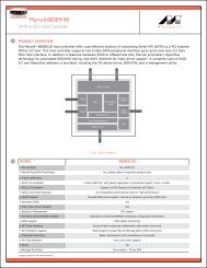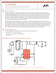
Marvell PXA27x Processor Family
PXA27x Design Guide - Marvell
PXA27x Design Guide - Marvell

Create successful ePaper yourself
Turn your PDF publications into a flip-book with our unique Google optimized e-Paper software.
<strong>PXA27x</strong> <strong>Processor</strong> <strong>Family</strong><br />
Design Guide<br />
5.3 Achieve Minimum Power Usage During All Power<br />
Modes<br />
Methods for achieving the lowest power usage during all power modes:<br />
• Connecting the crystal signals to an external differential oscillator achieves the least amount of power<br />
consumed by the <strong>PXA27x</strong> processor. Yet, the power consumed by the differential oscillator are considered for<br />
total system power usage. Exercise special care when selecting an external oscillator rather than an external<br />
crystal. Verify that the external oscillator is equally or more efficient than the <strong>PXA27x</strong> processor using a<br />
crystal.<br />
• Design the system so that all power domains uses the lower voltage level supported within the specifications,<br />
that is, VCC_MEM – 1.8 V.<br />
• Ensure I/O voltage levels track power domain levels, that is, for VCC_MEM – 1.8 V, all MD pins must drive at<br />
1.8 V, otherwise it could cause negative current.<br />
• Ideally, the system design allows measurements of power across all domains individually, helping the<br />
designer in isolating high current problems down to a specific voltage domain.<br />
• Disable all internal pull-ups/pull-downs on GPIO, which is accomplished through PTCR register settings.<br />
• Clearly define clock and memory controller settings.<br />
5.4 Achieve Minimum Power Usage During Deep Sleep<br />
Methods for achieving lowest power usage during deep sleep power modes:<br />
• Ground all non VCC_BATT power domains to enable the designer find the lowest power consumption and<br />
validate the design.<br />
• Monitor and register temperature sensitivity.<br />
• Ensure TDI and TMS pins are pulled high or left floating.<br />
• Ensure the USBC differential inputs (USBCP and USBCN) are pulled high or left floating with no impact to<br />
OTG pins.<br />
• Enable DC-DC internal power supply.<br />
• Ensure DC converter caps are connected properly.<br />
5.5 Achieve Minimum Power Usage During Sleep<br />
Methods used for achieving lowest power usage during sleep power modes:<br />
• Ground SRAM/PLL/Core power domains to enable the designer find the lowest power consumption and<br />
validate the design.<br />
• Configure GPIO signals of the <strong>PXA27x</strong> processor as input and drive a low from external source.<br />
Programmers can use PGSR/FS (GPIOs in O/P mode).<br />
• Ensure TDI and TMS pins are pulled high or left floating.<br />
• Ensure the USBC differential inputs (USBCP and USBCN) are pulled high or left floating with no impact to<br />
OTG pins.<br />
• Enable DC-DC internal power supply.<br />
5.6 Achieve Minimum Power Usage During Standby<br />
Methods used to achieve lowest power usage during standby power modes:<br />
• Ensure VCC_CORE and VCC_SRAM voltage is at 1.1 V.<br />
• Configure GPIO signals of the <strong>PXA27x</strong> processor as input and drive a low from external source.<br />
Programmers can use PGSR/FS (GPIOs in O/P mode).<br />
Doc. No. MV-S301207-00 Rev. A<br />
Page 46<br />
Copyright © 2009 <strong>Marvell</strong><br />
April 6, 2009, Released