Marvell PXA27x Processor Family
PXA27x Design Guide - Marvell
PXA27x Design Guide - Marvell

You also want an ePaper? Increase the reach of your titles
YUMPU automatically turns print PDFs into web optimized ePapers that Google loves.
<strong>PXA27x</strong> <strong>Processor</strong> <strong>Family</strong><br />
Design Guide<br />
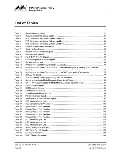
List of Tables<br />
Table 1: Related Documentation ................................................................................................................... 21<br />
Table 2: Recommended PCB Design Guidelines .......................................................................................... 25<br />
Table 3: PCB Dimensions for Copper-Defined Land Pads ............................................................................ 32<br />
Table 4: PCB Dimensions for Copper Defined Land Pads ............................................................................ 33<br />
Table 5: PCB Dimensions for Copper-Defined Land Pads ............................................................................ 34<br />
Table 6: External Power Supply Descriptions................................................................................................ 42<br />
Table 7: Clock Interface Signals .................................................................................................................... 53<br />
Table 8: Power Controller Interface Signals .................................................................................................. 54<br />
Table 9: DMA Interface Signals ..................................................................................................................... 63<br />
Table 10: Fly-By DMA Transfer Signals........................................................................................................... 65<br />
Table 11: Flow-Through DMA Transfer Signals............................................................................................... 66<br />
Table 12: Memory Address Map...................................................................................................................... 69<br />
Table 13: <strong>PXA27x</strong> <strong>Processor</strong> Memory Controller I/O Signals.......................................................................... 70<br />
Table 14: Minimum and Maximum Trace Lengths for the SDRAM Signals (Excluding SDCLK and<br />
SDCAS) ........................................................................................................................................... 74<br />
Table 15: Minimum and Maximum Trace Lengths for the SDCLK and SDCAS signals ............................ 75<br />
Table 16: SDRAM I/O Signals ......................................................................................................................... 77<br />
Table 17: SDRAM Memory Types Supported by <strong>PXA27x</strong> <strong>Processor</strong>.............................................................. 80<br />
Table 18: Normal and Alternate Mode Memory Address Signal Mapping ....................................................... 80<br />
Table 19: SA-1110 Address Compatibility Mode Memory Address Signal Mapping ....................................... 81<br />
Table 20: Flash Interface Signals ................................................................................................................... 83<br />
Table 21: ROM Interface Signals..................................................................................................................... 85<br />
Table 22: SRAM Interface Signals................................................................................................................... 86<br />
Table 23: VLIO Memory Interface Signals ....................................................................................................... 89<br />
Table 24: PC Card Interface Signals ............................................................................................................... 91<br />
Table 25: Alternate Bus Master Interface Signals............................................................................................ 97<br />
Table 26: LCD Interface Signal List ............................................................................................................... 102<br />
Table 27: LCD Controller Data Pin Utilization................................................................................................ 103<br />
Table 28: Passive Display Pins Required ...................................................................................................... 105<br />
Table 29: Passive Display Pins Required ...................................................................................................... 107<br />
Table 30: Passive Display Pins Required ...................................................................................................... 108<br />
Table 31: Passive Display Pins Required ...................................................................................................... 110<br />
Table 32: Passive Display Pins Required ...................................................................................................... 112<br />
Table 33: LCD Interface Signal List ............................................................................................................... 115<br />
Table 34: LCD Interface Signal List ............................................................................................................... 117<br />
Table 35: LCD Interface Signal List ............................................................................................................... 119<br />
Table 36: Active Display Pins Required......................................................................................................... 121<br />
Table 37: SSP Serial Port I/O Signals ........................................................................................................... 123<br />
Table 38: I2C Signal Description ................................................................................................................... 129<br />
Table 39: UART Signal Descriptions ............................................................................................................. 134<br />
Re<br />
Doc. No. MV-S301207-00 Rev. A<br />
Page 18<br />
Copyright © 2009 <strong>Marvell</strong><br />
April 6, 2009, Released