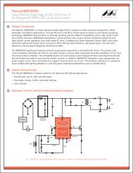
Marvell PXA27x Processor Family
PXA27x Design Guide - Marvell
PXA27x Design Guide - Marvell

Create successful ePaper yourself
Turn your PDF publications into a flip-book with our unique Google optimized e-Paper software.
<strong>PXA27x</strong> <strong>Processor</strong> <strong>Family</strong><br />
Design Guide<br />
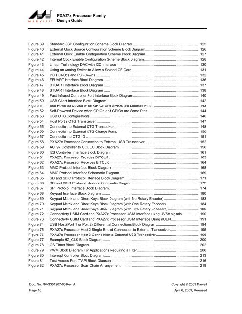
Figure 39: Standard SSP Configuration Scheme Block Diagram ................................................................... 125<br />
Figure 40: External Clock Source Configuration Scheme Block Diagram....................................................... 126<br />
Figure 41: External Clock Enable Configuration Scheme Block Diagram....................................................... 127<br />
Figure 42: Internal Clock Enable Configuration Scheme Block Diagram........................................................ 128<br />
Figure 43: Linear Technology DAC with I2C Interface.................................................................................... 130<br />
Figure 44: Using an Analog Switch to Allow a Second CF Card..................................................................... 131<br />
Figure 45: I 2 C Pull-Ups and Pull-Downs ......................................................................................................... 132<br />
Figure 46: FFUART Interface Block Diagram.................................................................................................. 136<br />
Figure 47: BTUART Interface Block Diagram ................................................................................................. 137<br />
Figure 48: STUART Interface Block Diagram ................................................................................................. 138<br />
Figure 49: Fast Infrared Controller Port Interface Block Diagram ................................................................... 140<br />
Figure 50: USB Client Interface Block Diagram .............................................................................................. 142<br />
Figure 51: Self Powered Device when GPIOn and GPIOx are Different Pins................................................. 143<br />
Figure 52: Self-Powered Device when GPIOn and GPIOx are Same Pins..................................................... 144<br />
Figure 53: USB OTG Configurations............................................................................................................... 146<br />
Figure 54: Host Port 2 OTG Transceiver ........................................................................................................ 147<br />
Figure 55: Connection to External OTG Transceiver ...................................................................................... 148<br />
Figure 56: Connection to External OTG Charge Pump................................................................................... 150<br />
Figure 57: Connection to OTG ID ................................................................................................................... 151<br />
Figure 58: <strong>PXA27x</strong> <strong>Processor</strong> Connection to External USB Transceiver ....................................................... 152<br />
Figure 59: AC ‘97 Controller to CODEC Block Diagram ................................................................................. 156<br />
Figure 60: I2S Controller Interface Block Diagram.......................................................................................... 161<br />
Figure 61: <strong>PXA27x</strong> <strong>Processor</strong> Provides BITCLK ............................................................................................ 163<br />
Figure 62: <strong>PXA27x</strong> <strong>Processor</strong> Receives BITCLK ........................................................................................... 164<br />
Figure 63: MMC Protocol Interface Block Diagram......................................................................................... 168<br />
Figure 64: MMC Protocol Interface Schematic Diagram................................................................................. 169<br />
Figure 65: SD and SDIO Protocol Interface Block Diagram............................................................................ 171<br />
Figure 66: SD and SDIO Protocol Interface Schematic Diagram.................................................................... 172<br />
Figure 67: SPI Protocol Interface Block Diagram............................................................................................ 174<br />
Figure 68: Keypad Interface Block Diagram ................................................................................................... 180<br />
Figure 69: Keypad Matrix and Direct Keys Block Diagram (with No Rotary Encoder).................................... 183<br />
Figure 70: Keypad Matrix and Direct Keys Block Diagram (with One Rotary Encoder).................................. 184<br />
Figure 71: Keypad Matrix and Direct Keys Block Diagram (with Two Rotary Encoders) ................................ 186<br />
Figure 72: Connectivity USIM Card and <strong>PXA27x</strong> <strong>Processor</strong> USIM Interface using UVSx signals.................. 190<br />
Figure 73: Connectivity USIM Card and <strong>PXA27x</strong> <strong>Processor</strong> USIM Interface Using nUEN............................. 191<br />
Figure 74: USB Host (Port 1 or Port 2) Differential Connections Block Diagram............................................ 194<br />
Figure 75: <strong>PXA27x</strong> <strong>Processor</strong> Host 2 Single-Ended Connection to External Transceiver.............................. 195<br />
Figure 76: <strong>PXA27x</strong> <strong>Processor</strong> Host 3 Connection to External USB Transceiver............................................ 196<br />
Figure 77: Example HZ_CLK Block Diagram.................................................................................................. 200<br />
Figure 78: OS Timer Block Diagram ............................................................................................................... 202<br />
Figure 79: PWM Block Diagram For Applications Requiring a Filter............................................................... 206<br />
Figure 80: Interrupt Controller Block Diagram................................................................................................. 213<br />
Figure 81: Test Access Port (TAP) Block Diagram ......................................................................................... 216<br />
Figure 82: <strong>PXA27x</strong> <strong>Processor</strong> Scan Chain Arrangement ............................................................................... 219<br />
Doc. No. MV-S301207-00 Rev. A<br />
Page 16<br />
Copyright © 2009 <strong>Marvell</strong><br />
April 6, 2009, Released