- Page 1 and 2: Cover Marvell ® PXA27x Processor F
- Page 3 and 4: Table of Contents Section 1. Introd
- Page 5 and 6: 5.5.1 Fly-By DMA Transfers ........
- Page 7 and 8: 7.5.8 Active Color, 18-bit per pixe
- Page 9 and 10: 15.4 Modes of Operation Overview ..
- Page 11 and 12: 24.2 Signals ......................
- Page 13 and 14: Appendix E. Companion Components fo
- Page 15 and 16: List of Figures Figure 1: PXA27x Pr
- Page 17 and 18: Figure 83: TAP Controller State Dia
- Page 19 and 20: Table 40: FFUART Interface Signals.
- Page 21 and 22: Section 1. Introduction to Part I T
- Page 23 and 24: 1.3 Package Introduction The PXA27x
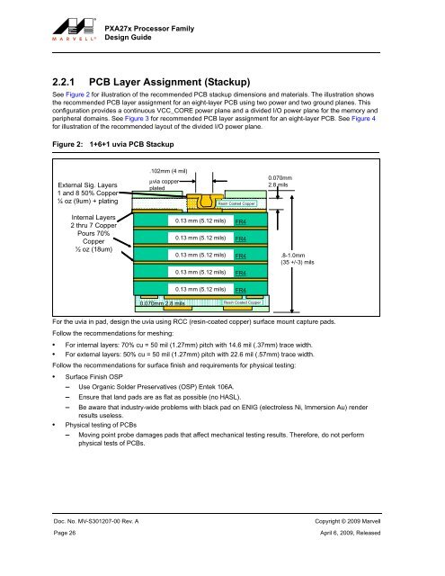
- Page 25: Section 2. PCB Design Guidelines Th
- Page 29 and 30: Figure 5: VF-BGA 13mm x 13mm Compon
- Page 31 and 32: Figure 7: PBGA 23mm x 23mm Componen
- Page 33 and 34: 2.2.3.2 FS-CSP Escape Routing This
- Page 35 and 36: Figure 10: Recommended Mobile Hands
- Page 37 and 38: Figure 11: FS-CSP (14x14) Tray Spec
- Page 39 and 40: Section 3. Design Check List For de
- Page 41 and 42: Section 4. Mixed Voltage Design Con
- Page 43 and 44: Figure 13: Minimal Voltage Regulato
- Page 45 and 46: Section 5. Power Measurements 5.1 O
- Page 47 and 48: • Ensure TDI and TMS pins are pul
- Page 49 and 50: Section 1. Introduction to Part II
- Page 51 and 52: Section 2. Package and Pins Refer t
- Page 53 and 54: Section 3. Clocks and Power Interfa
- Page 55 and 56: 3.2.3 Power Enable (PWR_EN) PWR_EN
- Page 57 and 58: Figure 14: Typical Battery and Exte
- Page 59 and 60: Note The oscillator-output-high-dri
- Page 61 and 62: Section 4. Internal SRAM There is n
- Page 63 and 64: Section 5. DMA Controller Interface
- Page 65 and 66: 5.5.1.1 Signals See Table 10 for th
- Page 67 and 68: Figure 18: Companion Chip Requestin
- Page 69 and 70: Section 6. System Memory Interface
- Page 71 and 72: Table 13: PXA27x Processor Memory C
- Page 73 and 74: Figure 18: General Memory Interface
- Page 75 and 76: Figure 19: PXA27x Processor Memory
- Page 77 and 78:
6.5 Modes of Operation Overview Ref
- Page 79 and 80:
Figure 22: SDRAM Memory System Exam
- Page 81 and 82:
Table 18: Device 1 x 12 x 8 BS0 A11
- Page 83 and 84:
Table 20: Signal Name Flash Interfa
- Page 85 and 86:
6.5.3 ROM Interface 6.5.3.1 ROM Sig
- Page 87 and 88:
Table 22: Signal Name SRAM Interfac
- Page 89 and 90:
6.5.5 Variable Latency Input/Output
- Page 91 and 92:
6.5.5.3 VLIO Memory Layout Notes Re
- Page 93 and 94:
Refer to Marvell ® PXA270 Processo
- Page 95 and 96:
Figure 28: External Logic for a Two
- Page 97 and 98:
esponsibility for SDRAM integrity d
- Page 99 and 100:
Figure 29: Alternate Bus Master Mod
- Page 101 and 102:
Section 7. LCD Interface This chapt
- Page 103 and 104:
Table 27: LCD Controller Data Pin U
- Page 105 and 106:
7.5 Modes of Operation Overview 7.5
- Page 107 and 108:
Table 29: Passive Display Pins Requ
- Page 109 and 110:
Table 30: Passive Display Pins Requ
- Page 111 and 112:
Table 31: Passive Display Pins Requ
- Page 113 and 114:
Table 32: Passive Display Pins Requ
- Page 115 and 116:
Table 33: LCD Interface Signal List
- Page 117 and 118:
7.5.7.1 Signals The signals in Tabl
- Page 119 and 120:
7.5.8.1 Signals The signals in Tabl
- Page 121 and 122:
7.5.9.1 Signals For active displays
- Page 123 and 124:
Section 8. SSP Port Interface 8.1 O
- Page 125 and 126:
Table 37: SSP Serial Port I/O Signa
- Page 127 and 128:
Figure 41: External Clock Enable Co
- Page 129 and 130:
Section 9. Inter-Integrated Circuit
- Page 131 and 132:
. Figure 44: Using an Analog Switch
- Page 133 and 134:
Section 10.UART Interfaces This cha
- Page 135 and 136:
Table 39: UART Signal Descriptions
- Page 137 and 138:
10.3.2 Bluetooth UART The BTUART is
- Page 139 and 140:
Section 11. Fast Infrared Interface
- Page 141 and 142:
Section 12.USB Client Controller Th
- Page 143 and 144:
• A more inexpensive solution is
- Page 145 and 146:
• During sleep and deep sleep mod
- Page 147 and 148:
Figure 54: Host Port 2 OTG Transcei
- Page 149 and 150:
• UDC • D+, D-, and transmit en
- Page 151 and 152:
Figure 57: Connection to OTG ID USB
- Page 153 and 154:
Table 47: Input from External USB T
- Page 155 and 156:
Section 13.AC ’97 This chapter de
- Page 157 and 158:
5. Enter sleep mode as outlined in
- Page 159 and 160:
Section 14.I 2 S Interface This cha
- Page 161 and 162:
Figure 60: I 2 S Controller Interfa
- Page 163 and 164:
Figure 61: PXA27x Processor Provide
- Page 165 and 166:
Section 15.MultiMediaCard/SD/SDIO C
- Page 167 and 168:
Table 54: MMC/SD/SDIO Controller Su
- Page 169 and 170:
See Figure 64 for the detailed sche
- Page 171 and 172:
Figure 65: SD and SDIO Protocol Int
- Page 173 and 174:
Table 58: SD/SDIO Card Pull-Up and
- Page 175 and 176:
See Figure 66 for illustration of a
- Page 177 and 178:
Section 16.Baseband Interface 16.1
- Page 179 and 180:
Section 17.Keypad Interface This ch
- Page 181 and 182:
17.4 Layout Notes This section has
- Page 183 and 184:
Figure 69: Keypad Matrix and Direct
- Page 185 and 186:
17.5.3 Keypad Matrix and Direct Key
- Page 187 and 188:
Section 18.USIM Controller Interfac
- Page 189 and 190:
18.2.2 USIM Card Interface Signals
- Page 191 and 192:
Figure 73: Connectivity USIM Card a
- Page 193 and 194:
Section 19.Universal Serial Bus Hos
- Page 195 and 196:
Figure 75: PXA27x Processor Host 2
- Page 197 and 198:
Section 20.Real Time Clock Interfac
- Page 199 and 200:
Section 21.OS Timer Interface This
- Page 201 and 202:
21.3.4 Output Control This block co
- Page 203 and 204:
Section 22.Pulse-Width Modulator In
- Page 205 and 206:
Section 23.General Purpose Input/Ou
- Page 207 and 208:
causes extraneous resets or interru
- Page 209 and 210:
Section 24.Interrupt Interface This
- Page 211 and 212:
Figure 80: Interrupt Controller Blo
- Page 213 and 214:
Section 25.JTAG Debug This chapter
- Page 215 and 216:
Table 69: TAP Controller Pin Defini
- Page 217 and 218:
Figure 82: PXA27x Processor Scan Ch
- Page 219 and 220:
Table 71: IEEE 1149.1 Boundary-Scan
- Page 221 and 222:
25.4.4.3 Data-Specific Registers Da
- Page 223 and 224:
25.4.5.3 Select-DR-Scan State The S
- Page 225 and 226:
25.4.5.14Pause-IR State The Pause-I
- Page 227 and 228:
Section 26.Quick Capture Interface
- Page 229 and 230:
Figure 85: Interface Options Summar
- Page 231 and 232:
Appendix A. PXA27x DVK Block Diagra
- Page 233 and 234:
Figure 87: Main Board Block Diagram
- Page 235 and 236:
Figure 89: Liquid Crystal Display B
- Page 237 and 238:
Figure 91: Keyboard Block Diagram F
- Page 239 and 240:
Appendix B. PXA27x Processor Develo
- Page 241 and 242:
Appendix C. PXA27x DVK Bill-of-Mate
- Page 243 and 244:
Appendix D. PXA27x Processor and PX
- Page 245 and 246:
DSADR16 - DSADR31 DTADR16 - DTADR31
- Page 247 and 248:
- FBR1-FBR6 registers added to supp
- Page 249 and 250:
• An optional output AC97_SYSCLK
- Page 251 and 252:
- The RTSR register has 12 new alar
- Page 253 and 254:
Note The only register that remains
- Page 255 and 256:
Appendix E. Companion Components fo
- Page 257 and 258:
E.6 Memory Controller E.7 LCD Contr
- Page 259 and 260:
E.13 AC ‘97 E.14 I 2 S (Inter IC
- Page 261 and 262:
Glossary 3G. An industry term used
- Page 263 and 264:
Circuit Switched. Used by wireless
- Page 265 and 266:
Endpoint Direction. The direction o
- Page 267 and 268:
HSTL. High-Speed Transceiver Logic
- Page 269 and 270:
inter-symbol interference, because
- Page 271 and 272:
SAW. Surface Acoustic Wave filter.
- Page 273 and 274:
TPV. Third Party Vendor Transaction
- Page 275:
Back Cover Marvell Semiconductor, I


