


You also want an ePaper? Increase the reach of your titles
YUMPU automatically turns print PDFs into web optimized ePapers that Google loves.
Rev 2.02<br />
E6A07<br />
In Figure E6-1, the schematic symbol for a PNP transistor is number 1.<br />
E6A08<br />
Alpha cutoff frequency indicates the frequency at which a transistor grounded base current gain has decreased to<br />
0.7 of the gain obtainable at 1 kHz.<br />
E6A09<br />
A depletion-mode FET is a FET that exhibits a current flow between source and drain when no gate voltage is<br />
applied.<br />
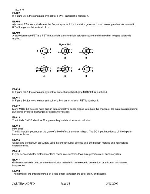
Figure E6-2<br />
E6A10<br />
In Figure E6-2, the schematic symbol for an N-channel dual-gate MOSFET is number 4.<br />
E6A11<br />
In Figure E6-2, the schematic symbol for a P-channel junction FET is number 1.<br />
E6A12<br />
Many MOSFET devices have built-in gate-protective Zener diodes to reduce the chance of the gate insulation being<br />
punctured by static discharges or excessive voltages.<br />
E6A13<br />
The initials CMOS stand for Complementary metal-oxide semiconductor.<br />
E6A14<br />
How does<br />
The DC input impedance at the gate of a field-effect transistor is high. The DC input impedance of the bipolar<br />
transistor is low.<br />
E6A15<br />
Silicon and germanium are widely used in semiconductor devices and exhibit both metallic and nonmetallic<br />
characteristics.<br />
E6A16<br />
P-type semiconductor material contains fewer free electrons than pure germanium or silicon crystals.<br />
E6A17<br />
Gallium arsenide is used as a semiconductor material in preference to germanium or silicon at microwave<br />
frequencies.<br />
E6A18<br />
The names of the three terminals of a field-effect transistor are gate, drain, and source.<br />
Jack Tiley <strong>AD7FO</strong> Page 54 3/15/2009