


You also want an ePaper? Increase the reach of your titles
YUMPU automatically turns print PDFs into web optimized ePapers that Google loves.
Rev 2.02<br />
E6B12<br />
Junction diodes are rated for maximum forward current and PIV (peak Inverse Voltage).<br />
E6B13<br />
A common use for PIN diodes is as an RF switch.<br />
E6B14<br />
Forward bias is required for an LED to produce luminescence.<br />
E6C Integrated circuits: TTL digital integrated circuits; CMOS digital integrated circuits; gates<br />
E6C01<br />
5 volts is the recommended power supply voltage for TTL series integrated circuits.<br />
E6C02<br />
The inputs of a TTL device assume a logic-high state if they are left open.<br />
E6C03<br />
The input voltage for a logic "high" in a TTL device operating with a positive 5-volt power supply is 2.0 to 5.5 volts.<br />
E6C04<br />
The input voltage for a logic "low" in a TTL device operating with a positive 5-volt power-supply is 0.0 to 0.8 volts.<br />
E6C05<br />
The advantage of CMOS logic devices over TTL devices is lower power consumption.<br />
E6C06<br />
Because the input switching threshold is about one-half the power supply voltage, CMOS digital integrated circuits<br />
have high immunity to noise on the input signal or power supply.<br />
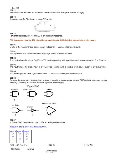
Figure E6-5<br />
And Gate Nand Gate<br />
Or Gate<br />
1 2 3<br />
Nor Gate<br />
4 5 6<br />
E6C07<br />
In Figure E6-5, the schematic symbol for an AND gate is number 1<br />
If inputs A and B are 1 then the output is 1.<br />
Input A Input B output<br />
0 0 0<br />
0 1 0<br />
1 0 0<br />
1 1 1<br />
Jack Tiley <strong>AD7FO</strong> Page 57 3/15/2009<br />
Nor Gate<br />
Inverter<br />
Inverter<br />
Operational Amp.<br />
Operational