


Create successful ePaper yourself
Turn your PDF publications into a flip-book with our unique Google optimized e-Paper software.
Rev 2.02<br />
E6C08<br />
In Figure E6-5, the schematic symbol for a NAND gate is number 2<br />
If not A and B are 1 then the output is 1.<br />
Input A Input B output<br />
0 0 0<br />
0 1 1<br />
1 0 1<br />
1 1 1<br />
E6C09<br />
In Figure E6-5, the schematic symbol for an OR gate is number 3.<br />
If either A or B input are 1 then the output is 1.<br />
Input A Input B output<br />
0 0 0<br />
0 1 1<br />
1 0 1<br />
1 1 1<br />
E6C10<br />
In Figure E6-5, the schematic symbol for a NOR gate is number 4.<br />
If neither A or B are 1 then the output will be 1.<br />
Input A Input B output<br />
0 0 1<br />
0 1 0<br />
1 0 0<br />
1 1 0<br />
E6C11<br />
In Figure E6-5, the schematic symbol for the NOT operation (inverter) is number 5.<br />
If the input is high the output is low, if the input is low the output will be high.<br />
Input Output<br />
0 1<br />
1 0<br />
E6D Optical devices and toroids: vidicon and cathode-ray tube devices; charge-coupled devices (CCDs);<br />
liquid crystal displays (LCDs); toroids: permeability, core material, selecting, winding<br />
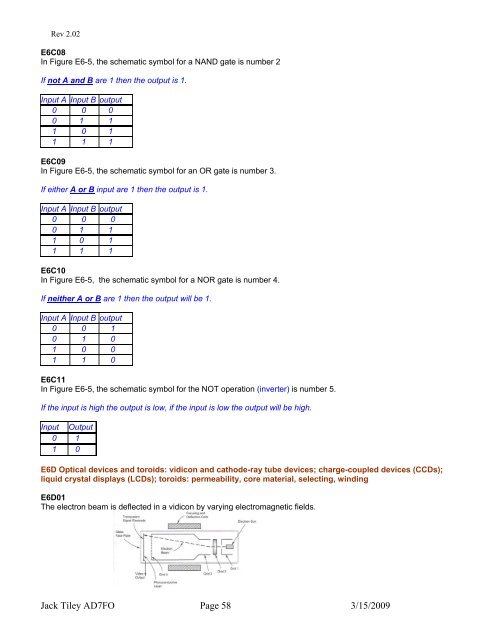
E6D01<br />
The electron beam is deflected in a vidicon by varying electromagnetic fields.<br />
Jack Tiley <strong>AD7FO</strong> Page 58 3/15/2009