ZX Computings - OpenLibra
ZX Computings - OpenLibra
ZX Computings - OpenLibra

Create successful ePaper yourself
Turn your PDF publications into a flip-book with our unique Google optimized e-Paper software.
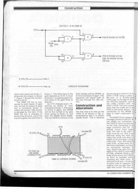
0 VOLTS- PIN 7<br />
Construction<br />
GATES 1-4 IN 7400 IC<br />
+5 VOLTS- PIN 14 CIRCUIT DIAGRAM<br />
when both inputs are binary 1,<br />
otherwise the output is binary<br />
1. Figure 1 shows the connections<br />
to the IC.<br />
The RAM CS line is connected<br />
to both inputs of gate<br />
one, so that its output of gate<br />
one is constantly binary 0,<br />
unless the correct 1 6K section<br />
is decoded by the ULA. If the<br />
RAM CS line is changed to<br />
binary 0 by the ULA, one of the<br />
inputs to gates two and three is<br />
+5 VOLTS<br />
TO PAD 2A<br />
ON EDGE<br />
CONNECTOR<br />
13<br />
binary 1. The other input to the<br />
gate depends on A1 0. It must<br />
be binary 1 to operate gate two,<br />
and binary 0 for gate three to<br />
operate.<br />
As A10 changes'every 1K,<br />
starting as binary 0, then<br />
changing to binary 1, then back<br />
to binary 0 again, the ORAM<br />
will be first turned on by gate<br />
three going to binary 0, and<br />
then the ERAM (Extra RAM),<br />
The next RAM to come on in the<br />
A10<br />
7400 IC (UPSIDE DOWN}<br />
third change will be ORAM, as<br />
A10 is now binary 0 again. This<br />
sequence will repeat itself all<br />
the way through the 16K section.<br />
Construction and<br />
Alterations<br />
The first step is to wire up the<br />
7400 IC as shown in Fig. 2,<br />
remembering that it is shown<br />
upside down. This is because<br />
ORAM CS<br />
0 VOLTS<br />
ERAM CS<br />
we are going to mount it on tN je<br />
<strong>ZX</strong>81 's PCB using a piece a p<br />
Blu-tack or a double side<<br />
sticky pad, so the legs of the IC<br />
are sticking upwards, and cfe<br />
not make contact with tto<br />
<strong>ZX</strong>B1 's PCB. The only connec<br />
tions that are made are to th»<br />
PCB at the points shown. Th<br />
connection to the ORAM C!<br />
lines is made underneath th<br />
PCB.<br />
The RAM CS line appears o<br />
the edge connector pad 2 A, Wcan<br />
solder our connection n<br />
the 7400 IC (pins one and twc<br />
to the hole connected to th<br />
o<br />
h<br />
u<br />
c<br />
$<br />
c<br />
ir<br />
lr<br />
C<br />
edge connector pad 2A. Th g<br />
printed circuit track leadini „<br />
from this pad to pin eight c v<br />
lC4b must be cut. Pick a spo £<br />
half-way along the track an t)<br />
make two small cuts about a a<br />
eighth of an inch apart, using f(<br />
craft knife. Then, still using th g<br />
craft knife, scrape away all c<br />
the track in between, sotherei n<br />
no connection between th t)<br />
two. Attach the wire from pi e<br />
eight of the 7400 IC to pin eigf c<br />
of IC4b, whether fitted or n