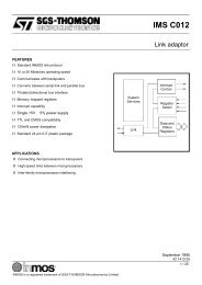
1993_Motorola_Linear_Interface_ICs_Vol_2.pdf
1993_Motorola_Linear_Interface_ICs_Vol_2.pdf
1993_Motorola_Linear_Interface_ICs_Vol_2.pdf

You also want an ePaper? Increase the reach of your titles
YUMPU automatically turns print PDFs into web optimized ePapers that Google loves.
Glitch Area - The energy content of a glitch, specifically<br />
In volt-seconds. It is the area under the curve of the glitch<br />
waveform. For a symmetrical glitch, the area and the energy<br />
can be zero.<br />
Gray Code - Also known as reflected binary code, it is a<br />
digital code such that each code differs from adjacent codes<br />
by only one bit. Since more than one bit is never changed<br />
at each transition, race condition errors are eliminated.<br />
Integral Nonlinearity - The maximum error of an ND or<br />
DAC, transfer function from the ideal straight line connecting<br />
the analog end points. This parameter is sensitive to<br />
dynamics, and test conditions must be specified in order to<br />
be meaningful. This parameter is the best overall indicator<br />
of the device's performance.<br />
LSB - Least Significant Bit. It is the lowest order bit of a<br />
binary code.<br />
Line Regulation - The ability of a voltage regulator to<br />
maintain a certain output voltage as the input to the regulator<br />
is varied. The error is typically expressed as a percent of<br />
the nominal output voltage.<br />
Load Regulation - The ability of a voltage regulator to<br />
maintain a certain output voltage as the load current is varied.<br />
The error is typically expressed as a percent of the nominal<br />
output voltage.<br />
Monotonlclty - The characteristic of the transfer function<br />
whereby increasing the input code (of a DAC), or the input<br />
Signal (of and ND), results in the output never decreasing.<br />
Nonmonotonicity occurs if the differential nonlinearity<br />
exceeds ± 1 LSB.<br />
MSB - Most Significant Bit. It is the highest order bit of a<br />
binary code.<br />
Natural Binary Code - A binary code defined by:<br />
N = An2n + ... + Aa23 + A222 + A121 + A020<br />
where each "A" coefficient has a value of 1 or O. Typically,<br />
all zeros correspond to a zero input voltage of an ND, and<br />
all ones correspond to the most positive Input voltage.<br />
Nyquist Theory - See Sampling Theorem.<br />
Offset Binary Code - Applicable only to bipolar input (or<br />
output) data converters, it is the same as Natural Binary<br />
code, except that all zeros correspond to the most negative<br />
output signal (of a D/A), while all ones correspond to the<br />
most positive output. .<br />
MC10322<br />
Output Compliance - The maximum voltage range to which<br />
the DAC outputs can be subjected, and still meet all<br />
specifications.<br />
Power Supply Rejection Ratio - The ability of a device<br />
to reject noise andlor ripple on the power supply pins from<br />
appearing at the outputs. An AC measurement, this<br />
parameter is usually expressed in dB rejection.<br />
Power Supply Sensitivity - The change in a data<br />
converter's performance with changes in the power supply<br />
voltage(s). This parameter is usually expressed in percent<br />
of full scale versus t.v.<br />
'Propagation Delay - For a DAC, the time from when the<br />
clock input crosses its threshold to when the DAC output(s)<br />
changes.<br />
Quantltlzatlon Error - Also known as digitization error or<br />
uncertainty. It is the inherent error involved in digitizing an<br />
analog signal due to the finite number of steps at the digital<br />
output versus the infinite number of values at the analog<br />
input. This error is a minimum of ± 1/2 LSB.<br />
Resolution - The smallest change which can be discerned<br />
by an ND converter, or produced by a DAC. It is usually<br />
expressed as the number of bits (n), where the converter<br />
has 2n possible states.<br />
Sampling Theorem - Also known as the Nyquist Theorem.<br />
It states that the sampling frequency of an ND must be no<br />
less than 2x the highest frequency (of interest) of the analog<br />
signal to be digitized in order to preserve the information of<br />
that analog signal.<br />
Settling Time - For a DAC, the time required for the output<br />
to change (and settle in) from an initial ±1/2 LSB error band<br />
to the final ± 112 LSB error band.<br />
TTL - Transistor-transistor logic,<br />
Two's Complement Code - A binary code applicable to<br />
bipolar operation, in which the positive and negative codes<br />
of the same analog magnitude sum to all zeros, plus a carry.<br />
It is the same as offset binary code, with the MSB inverted.<br />
Unipolar Input - A mode of operation whereby the analog<br />
input range (of an ND), or output range (of a D/A), includes<br />
values of a single polarity. Examples are:<br />
o to +10 V, 0 to -5.0 V, +2.0 V to + 8.0 V, etc.<br />
Acldltlonallnfonnatlon regarding the trensmlsslon characteristics 01 PC board treeks can be found In<br />
<strong>Motorola</strong>'s MECL System Daslgn Handbook (HB205).<br />
MOTOROLA LINEAR/INTERFACE <strong>ICs</strong> DEVICE DATA<br />
6-77