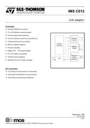
1993_Motorola_Linear_Interface_ICs_Vol_2.pdf
1993_Motorola_Linear_Interface_ICs_Vol_2.pdf
1993_Motorola_Linear_Interface_ICs_Vol_2.pdf

You also want an ePaper? Increase the reach of your titles
YUMPU automatically turns print PDFs into web optimized ePapers that Google loves.
used) and at what current levels they are operating. The<br />
maximum power which may be dissipated within the package<br />
is determined by:<br />
PDmax= TJmax-TA<br />
Rcj>JA<br />
where: RaJA = package thermal resistance (typ.<br />
70°C/W for the DIP package, 85°C/W for<br />
SOIC package);<br />
T Jmax = max. operating junction<br />
temperature, and<br />
TA = ambient temperature.<br />
Since the thermal shutdown feature has a trip point of<br />
+ 150°C, ± 20°C, T Jmax is selected to be + 130°C. The power<br />
dissipated within the package is calculated from:<br />
PD = {[(VCC - VOH) • IOHI + VOL· loll} each driver<br />
+ (VCC • ICC)<br />
where: VCC = the supply voltage;<br />
VOH, VOL are measured or estimated from<br />
Figures 7 to 10;<br />
ICC = the quiescent power supply current<br />
(typ. 60 rnA).<br />
As indicated in the equation, the first term (in brackets) must<br />
be calculated and summed for each of the four drivers, while<br />
the last term is common to the entire package.<br />
Example 1 :TA = +25°C, IOl = IOH = 55 rnA for each driver,<br />
VCC= 5.0 V, DIP package. How many drivers per package can<br />
be used?<br />
Maximum allowable power dissipation is:<br />
PDmax=<br />
Since the power supply current of 60 rnA dissipates 300<br />
mW, that leaves 1.2 W (1 .5 W - 0.3 W) for the drivers. From<br />
Figures 7 and 9, VOL =1.75 V, and VOH =3.85 V. The power<br />
dissipated in each driver is:<br />
{(5.0 - 3.85) • 0.055} + (1.75 • 0.055) = 160 mW.<br />
Since each driver dissipates 160 mW, the four drivers per<br />
package could be used in this application<br />
Example 2:TA = +85°C, IOl = 27.8 rnA, IOH = 20 rnA for<br />
each driver, VCC = 5.0 V, SOIC package. How many drivers<br />
per package can be used?<br />
Maximum allowable power dissipation is:<br />
PDmax=<br />
Since the power supply current of 60 rnA dissipates 300<br />
mW, that leaves 230 mW (530 mW - 300 mW) for the drivers.<br />
From Figures 8 and 10 (adjusted for VCC =5.0V), VOl=I.38<br />
V, and VOH =4.27 V. The power dissipated in each driver is:<br />
{(5.0 - 4.27) • 0.020} + (1.38 • 0.0278) = 53 mW<br />
Since each driver dissipates 53 mW, the use of all four<br />
drivers in a package would be marginal. Options include<br />
reducing the load current, reducing the ambient temperature,<br />
and/or providing a heat sink.<br />
MC75172B, MC75174B<br />
System Requirements<br />
EIA-485 requires each driver to be capable of<br />
transmitting data differentially to at least 32 unit loads, plus an<br />
equivalent DC termination resistance of 60Q, over a common<br />
mode voltage of -7.0 to + 12 V. A unit load (U.L.), as defined<br />
by EIA-485, is shown in Figure 17.<br />
Figure 17. Unit load Definition<br />
Reprinted from BA-4B5. Electronic Industries Association,<br />
Washington,DC.<br />
MOTOROLA LINEAR/INTERFACE <strong>ICs</strong> DEVICE DATA<br />
7-190<br />
A load current within the shaded regions represents an<br />
impedance of less than one U.L., while a load current of a<br />
magnitude outside the shaded area is greater than one U.L. A<br />
system's total load is the sum of the unit load equivalents of<br />
each receiver's input current, and each disabled driver's<br />
output leakage current. The 60Q termination resistance<br />
mentioned above allows for two 120Q terminating resistors.<br />
Using the EIA·485 requirements (worst case limits), and<br />
the graphs of Figures 7 and 9, it can be determined that the<br />
maximum current an MC75172B or (MC75174B) driver will<br />
source or sink is =65 rnA.<br />
System Example<br />
An example of a typical EIA·485 system is shown in<br />
Figure 18. In this example, it is assumed each receiver'S input<br />
characteristics correspond to 1.0 U.L. as defined in Figure 17.<br />
Each "off' driver, with a maximum leakage of ±50 I1A over the<br />
common mode range, presents a load of =0.06 U.L. The total<br />
load for the active driver is therefore 8.3 unit loads, plus the<br />
parallel combination of the two terminating resistors (60Q). It<br />
is up to the system software to control the driver Enable pins<br />
to ensure that only one driver is active at any time.<br />
Termination Resistors<br />
Transmission line theory states that, in order to preserve<br />
the shape and integrity of a waveform traveling along a cable,<br />
the cable must be terminated in an impedance equal to its<br />
characteristic impedance. In a system such as that depicted<br />
in Figure 18, in which data can travel in both directions, both<br />
physical ends of the cable must be terminated. Stubs, leading<br />
to each receiver and driver, should be as short as possible.<br />
leaving off the terminations will generally result in<br />
reflections which can have amplitudes of several volts above<br />
Vccorbelowground. These overshoots and undershoots can<br />
disrupt the driver and/or receiver operation, create false data,<br />
and in some cases damage components on the bus.