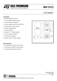
1993_Motorola_Linear_Interface_ICs_Vol_2.pdf
1993_Motorola_Linear_Interface_ICs_Vol_2.pdf
1993_Motorola_Linear_Interface_ICs_Vol_2.pdf

Create successful ePaper yourself
Turn your PDF publications into a flip-book with our unique Google optimized e-Paper software.
<strong>Vol</strong>tage outputs of a larger magnitude are obtainable with this<br />
circuit which uses an external operational amplifier as a current<br />
to voltage converter. This configuration automatically keeps the<br />
output of the MC1408 at ground potential and the operational<br />
amplifier can generate a positive voltage limited only by its positive<br />
supply voltage. Frequency response and settling time are primarily<br />
determined by the characteristics of the operational amplifier. In<br />
addition, the operational amplifier must be compensated for unity<br />
gain, and in some cases overcompensation may be desirable.<br />
Note that this configuration results in a positive output voltage<br />
only, the magnitude of which is dependent on the digital input.<br />
The following circuit shows how the MLM301AG can be used<br />
in a feedforward mode resulting in a full scale settling time on<br />
the order of 2.0 ,,",S.<br />
(To pin 4<br />
of MC15D8LBI<br />
FIGURE 18<br />
65 pF<br />
5.1 k.<br />
MC1408, MC1508<br />
APPLICATIONS INFORMATION (continued)<br />
--o--+.--oVQ<br />
An alternative method is to use the MC1539G and input compensation.<br />
Response of this circuit is also on the order of 2.0 ,,",S.<br />
See <strong>Motorola</strong> Application Note AN-459 for more details on this<br />
concept.<br />
FIGURE 19<br />
+15 V<br />
-15 V<br />
35 pF<br />
5 k<br />
10 k<br />
MOTOROLA LINEAR/INTERFACE <strong>ICs</strong> DEVICE DATA<br />
6-23<br />
The positive voltage range may be extended by cascading the<br />
output with a high beta common base transistor, Q 1, as shown.<br />
FIGURE 20 - EXTENDING POSITIVE<br />
VOLTAGE RANGE<br />
Vee<br />
5 k<br />
Go<br />
(Resistor and<br />
diode optional.<br />
see toxt)<br />
The output voltage range for this circuit is 0 volts to BVCBO<br />
of the transistor. If pin 1 is left open, the transistor base may be<br />
grounded, eliminating both the resistor and the diode. Variations<br />
in betil must be considered for wide temperature range applications.<br />
An inverted output waveform may be obtained by using a<br />
load resistor from a positive reference voltage to the collector of<br />
the transistor. Also, high-speed operation is possible with a large<br />
output voltage swing, because pin 4 is held at a constant voltage.<br />
The resistor (RI to VEE maintains the transistor emitter voltage<br />
when all bits are "off" and insures fast turn-on of the least<br />
significant bit.<br />
Combined Output Amplifier and <strong>Vol</strong>tage Reference<br />
For many of its applications the MC1408 requires a reference<br />
voltage and an operational amplifier. Normally the operational<br />
amplifier is used as a current to voltage converter and its output<br />
need only go positive. With the popular MC1723G voltage regulator<br />
both of these functions are provided in a single package with<br />
the added bonus of up to 150 mA of output current. See Figure<br />
21. The MC1723G uses both a positive and negative power supply.<br />
The reference voltage of the MC1723G is then developed with<br />
respect to the negative voltage and appears as a common-mode<br />
signal to the reference amplifier in the D-to-A converter. This<br />
allows use of its output amplifier as a classic current-to-voltage<br />
converter with the non-inverting input grounded.<br />
Since ±15 V and +5.0 V arc normally available in a combination<br />
digital-to-analog system, only the -5.0 V need be developed.<br />
A resistor divider is sufficiently accurate since' the allowable range<br />
on pin 5 is from -2.0 to -8.0 volts. The 5.0 kilohm pull down<br />
resistor on the ampl ifier output is necessary for fast negative<br />
transitions.<br />
Full scale output may be increased to as much as 32 volts by<br />
increasing RO and raising the +15 V supply voltage to 35 V maximum.<br />
The resistor divider should be altered to comply with the<br />
maximum limit of 40 volts across the MC1723G. Co may be<br />
decreased to maintain the same RaCa product if maximum speed<br />
is desired.