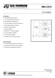
1993_Motorola_Linear_Interface_ICs_Vol_2.pdf
1993_Motorola_Linear_Interface_ICs_Vol_2.pdf
1993_Motorola_Linear_Interface_ICs_Vol_2.pdf

Create successful ePaper yourself
Turn your PDF publications into a flip-book with our unique Google optimized e-Paper software.
10. Calculate the shorted load average power dissipation for<br />
the application using Equations 8 and 9. This involves<br />
determining the peak shorted load power dissipation of the<br />
TMOS device and gate duty cycle. The duty cycle is based<br />
on VDS(min), the value of VDS under shorted conditions (Le.<br />
Vbat(max))·<br />
11. The calculated shorted load average power dissipation<br />
of Step 1 0 should be less than the maximum power<br />
dissipation under normal operating conditions calculated in<br />
Step 4. If this is not the case, there are two options.<br />
Option one is to reduce the thermal resistance of the TMOS<br />
device heatsink, in other words, use a larger or better heatsink.<br />
This though, is not always practical to do particularly if<br />
restricted by size.<br />
Option two is to set VDS(min) to the lowest practical value.<br />
If for instance VDS(min) is set to 4.0 V when only 2.0 V are<br />
needed, the short circuit duty cycle will be over twice as large,<br />
resulting in double the TMOS device power dissipated.<br />
Keeping VDS(min) to a minimum, reduces the shorted load<br />
average power.<br />
12. Choose a value of CT. The value of CT can be determined<br />
either by trial and error or by characterizing the VDS waveform<br />
for the load and selecting a capacitor value that generates<br />
a minimum fault time curve (see Equation 4) that<br />
encompasses the VDS versus time waveform. The value of<br />
CT has no effect on the duty cycle itself as was pointed out<br />
earlier. See Figure 23 for a graphical selection of CT.<br />
Inductive Loads<br />
The TMOS device is turned off by pulling the gate to near<br />
ground potential. Turning off an inductive load will cause<br />
the source of the TMOS device to go below ground due to<br />
flyback voltage to the point where the TMOS device may<br />
become biased on again allowing the inductive energy to be<br />
dissipated through the load. There is an internal 14 V zener<br />
diode clamp from the gate to source pin which will limit how far<br />
the source pin can be pulled below ground. For high inductive<br />
loads, it may be necessary to have an external 10k current<br />
limiting resistor in series with the source pin to limit the clamp<br />
current in the event the source pin is pulled more than 14 V<br />
below ground.<br />
Transient Faults<br />
The MC33091 is not able to withstand automotive voltage<br />
transients directly. However, by correctly sizing resistor RS<br />
and capacitor CS, the MC33091 can withstand load dump<br />
and other automotive type transients. The VCC voltage is<br />
clamped at approximately 30 V through the use of an internal<br />
zener diode.<br />
Under reverse battery conditions, the load will be energized<br />
in reverse due to the parasitic body diode inherent in the<br />
TMOS device. Under this condition, the drain is grounded and<br />
the MC33091 clamps the gate at 0.7 V below the battery<br />
potential. This turns the TMOS device on in reverse and<br />
MC33091<br />
MOTOROLA LINEAR/INTERFACE <strong>ICs</strong> DEVICE DATA<br />
10-52<br />
minimizes the voltage across the TMOS device resulting in<br />
minimal power dissipation. Neither the MC33091 nor the<br />
TMOS device will be damaged under such a condition. In<br />
addition, if the load can tolerate a reverse polarity, the load will<br />
not be damaged. Some sensitive applications may not tolerate<br />
a reverse polarity load condition with reverse battery polarity.<br />
There is no protection of the TMOS device during a reverse<br />
battery condition if the load itself is already shorted to ground.<br />
The MC33091 will not incur damage under this specialized<br />
reverse battery condition but the TMOS device may be<br />
damaged since there could be significant energy available<br />
from the battery to be dissipated in the TMOS device.<br />
The MC33091 will withstand a maximum VCC voltage of<br />
28 V and with the proper TMOS device used, the system can<br />
withstand a double battery condition.<br />
Figure 32 depicts a method of protecting the FET from<br />
positive transient voltages in excess of the rated FET<br />
breakdown <strong>Vol</strong>tage. The zener voltage, in this case, should be<br />
less than the FET breakdown voltage. The diode D is<br />
necessary where reverse battery protection is required to<br />
protect the gate of the FET.<br />
EMI Concern<br />
The gate capacitance and thus the size of the TMOS device<br />
used will determine the turn-on and turn-off times<br />
experienced. In a practical sense, smaller TMOS devices<br />
have smaller gate capacitances and give rise to higher slew<br />
rates. By way of example, the slew rate of an MPT50N06<br />
TMOS device might be of the order of 7.5115 while that of an<br />
MPT8N10 is23 115 (see Figure 13). The slew rate, or speed of<br />
turn-on or turn-off can be calculated by assuming the charge<br />
pump to supply approximately 100 !!A over the time the gate<br />
capacitance will transition a VGS voltage of 0 V to 10 V. In<br />
reality, the VGS voltage will be greater than 10 V but the<br />
additional increase in TMOS drain current will be minimal for<br />
V GS voltages greater than 10 V.<br />
Sizing of the charge pump current is such that slew rate<br />
need not be of concern in all but the most critical of<br />
applications. Where limiting of EMI is of concern, the charge<br />
pump of the MC33091 may be slew rate limited by adding an<br />
external feedback capacitor from the gate to source of the<br />
TMOS device for slow down adjustment of both turn-on and<br />
turn-off times (see Figure 29). Figures 27 through 31 depict<br />
various methods of modifying the turn-on or turn-off times.<br />
Figure 31 depicts a method of using only six external<br />
components to decrease turn-off time and clamp the fiyback<br />
voltage associated with inductive loads. VGS(th) used in the<br />
critical component selection criteria refers to the gate to source<br />
threshold voltage of the FET used in the application.<br />
Caution should be exercised when slowing down the<br />
switching transition time since doing 50 can greatly increase<br />
the average power dissipation of the TMOS device. The<br />
resulting increase in power dissipation should be taken into<br />
account when selecting the RTCT time constant values<br />
in order to protect the TMOS device from any over<br />
current condition.