- Page 1 and 2:
Copyright Library of Congress Catal
- Page 3 and 4:
National Improvements | Virtual Ins
- Page 5 and 6:
formulations, the results from Math
- Page 7 and 8:
Hardware and Software Requirements
- Page 9 and 10:
Chan0_out Pin 21 Chan0_in Pin 68 Gn
- Page 11 and 12:
LabVIEW VI Libraries and Project an
- Page 13 and 14:
1.1 Resistor Voltage Divider and MO
- Page 15 and 16:
1.3 Frequency Response of the Ampli
- Page 17 and 18:
At f = flo, . This, by definition,
- Page 19 and 20:
1.5 Exercises and Projects Project
- Page 21 and 22:
2.1 BJT and MOSFET Schematic Symbol
- Page 23 and 24:
2.2 Fundamentals of Signal Amplific
- Page 25 and 26:
2.3 Basic NMOS Common-Source Amplif
- Page 27 and 28:
Using (2.4), (2.5), (2.9), and (2.1
- Page 29 and 30:
2.6 Exercises and Projects Project
- Page 31 and 32:
Unit 3. Characterization of MOS Tra
- Page 33 and 34:
In electronic circuit applications,
- Page 35 and 36:
The output-characteristic equation
- Page 37 and 38:
Equation 3.11 From the data measure
- Page 39 and 40:
The input circuit loop equation (Fi
- Page 41 and 42:
which leads to the result (3.5), re
- Page 44 and 45:
3.6 Exercises and Projects Project
- Page 46 and 47:
Unit 4. Signal Conductance Paramete
- Page 48 and 49:
4.2 Transistor Variable Incremental
- Page 50 and 51:
4.3 Transconductance Parameter The
- Page 52 and 53:
4.4 Body-Effect Transconductance Pa
- Page 54 and 55:
4.5 Output Conductance Parameter Th
- Page 56 and 57:
With a 1 - V drop across RS and a 5
- Page 58 and 59:
By the nature of the load-line func
- Page 60 and 61:
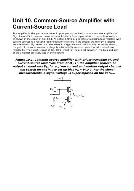
Unit 5. Common-Source Amplifier Sta
- Page 62 and 63:
5.2 Amplifier Voltage Gain This dc
- Page 64 and 65:
etween the drain and source of the
- Page 66 and 67:
5.3 Linearity of the Gain of the Co
- Page 68 and 69:
where av Vds/Vgs and where the appr
- Page 70 and 71:
is attached directly to the gate. B
- Page 72 and 73:
5.5 Design of a Basic Common-Source
- Page 74 and 75:
= VGSo - Vtno at the high and low e
- Page 76 and 77:
RG can be selected somewhat arbitra
- Page 78 and 79: 5.7 Exercises and Projects Project
- Page 80 and 81: 6.1 Grounded-Source Amplifier: Coup
- Page 82 and 83: and Equation 6.6 Note that the "RC"
- Page 84 and 85: 6.4 Load Coupling Capacitor The com
- Page 87 and 88: 6.5 Summary of Equations MOSFET cou
- Page 89 and 90: Unit 7. MOSFET Source-Follower Buff
- Page 91 and 92: 7.2 Source-Follower Voltage Transfe
- Page 93 and 94: 7.3 Body Effect and Source-Follower
- Page 95 and 96: 7.4 Summary of Equations Threshold
- Page 97 and 98: Unit 8. MOSFET Differential Amplifi
- Page 99 and 100: 8.2 DC Imbalances In a real transis
- Page 101 and 102: 8.3 Signal Voltage Gain of the Idea
- Page 103 and 104: 8.4 Effect of the Bias Resistor on
- Page 105 and 106: 8.5 Differential Voltage Gain Suppo
- Page 107 and 108: 8.7 Voltage Gains Including Transis
- Page 109 and 110: 8.7.2 Common-Gate Amplifier Stage T
- Page 111 and 112: with RD1 = RD2 and gm1 = gm2. In th
- Page 113 and 114: It follows that the gain for the in
- Page 115 and 116: 8.9 Amplifier Gain with Differentia
- Page 117 and 118: 8.11 Summary of Equations Rs = Ris2
- Page 119 and 120: 8.12 Exercises and Projects Project
- Page 121 and 122: 9.1 Basic Current Source An example
- Page 123 and 124: 9.2 Current Source with Source Dege
- Page 125 and 126: If the magnitude of the voltage acr
- Page 127: Any slight possible difference in
- Page 131 and 132: 10.2 Signal Voltage Gain The expres
- Page 133 and 134: 10.3 Summary of Equations Output dr
- Page 135 and 136: Unit 11. Operational Amplifiers wit
- Page 137 and 138: 11.1.1 Voltage Gain of the Noninver
- Page 139 and 140: This expression can be manipulated
- Page 141 and 142: 11.3 Operational Amplifier Offset I
- Page 143 and 144: where the approximation usually app
- Page 145 and 146: where Avo is the amplifier gain at
- Page 147 and 148: 11.7 Exercises and Projects Project
- Page 149 and 150: 12.1 Operational Amplifier Integrat
- Page 151 and 152: This demonstrates that for the circ
- Page 153 and 154: with a steady-state value of Vop. A
- Page 155 and 156: Equation 12.25 A good estimate come
- Page 157 and 158: 12.4 Exercises and Projects Project
- Page 159 and 160: 13.1 Combining NMOS and PMOS Circui
- Page 161 and 162: 13.3 Stabilization of Signal Gain a
- Page 163 and 164: An estimate of the new output volta
- Page 165 and 166: This produces (9.9) from Ro = Vo/Io
- Page 167 and 168: Equation 13.13 where 13.12 has been
- Page 169 and 170: The open-loop transconductance is G
- Page 171 and 172: Unit 14. Development of a Basic CMO
- Page 173 and 174: 14.2 Current-Source Output Resistan
- Page 175 and 176: 14.3 Current-Source Load for the Co
- Page 177 and 178: 14.4 Current-Source Load for the Di
- Page 179 and 180:
the node (exclusive of the separate
- Page 181 and 182:
14.5 Two-Stage Amplifier with Curre
- Page 183 and 184:
14.6 Output Buffer Stage It is evid
- Page 185 and 186:
Suppose that ID6 = 400 µA, W6 = 50
- Page 187 and 188:
Av and Ro are calculated once, usin
- Page 189 and 190:
Since the source follower of M1 has
- Page 191 and 192:
14.9 Summary of Equations CMRR = 1
- Page 193:
Unit A. Communicating with the Circ
- Page 196 and 197:
Place AI Acquire Waveform.vi in the
- Page 198 and 199:
Click from the Front Panel or Diagr
- Page 200 and 201:
Now go to the Diagram (under Menu W
- Page 202 and 203:
To complete connections to the term
- Page 204 and 205:
Now use the Edit Text Tool to edit
- Page 206 and 207:
on the left in the diagram . The Wh
- Page 208 and 209:
Figure A.15. Frame of Sequence Stru
- Page 210 and 211:
The transition regions are nonabrup
- Page 212 and 213:
during the oscilloscope measurement
- Page 214 and 215:
Unit B. Characterization of the Bip
- Page 216 and 217:
junction diodes, the current is lar
- Page 218 and 219:
common to the input and output and
- Page 220 and 221:
B.2 Base-Width Dependence on Juncti
- Page 222 and 223:
Figure B.8. Diodelike characteristi
- Page 224 and 225:
The minus sign comes from having as
- Page 226 and 227:
Figure B.10. Circuit for measuring
- Page 228 and 229:
B.5 Output Characteristics of BJT i
- Page 230 and 231:
After measuring the output characte
- Page 232 and 233:
B.6 SPICE Solution for IC versus VC
- Page 234 and 235:
B.7 Collector-Emitter Voltage and C
- Page 236 and 237:
B.8 DC as a Function of Collector C
- Page 238 and 239:
B.10 Summary of Equations Common-em
- Page 240 and 241:
Unit C. Common-Emitter Amplifier St
- Page 242 and 243:
The equation set above has three un
- Page 244 and 245:
The output-resistance parameter, ro
- Page 246 and 247:
of βDC as possible. Signal paramet
- Page 248 and 249:
Equation C.17 We note that the magn
- Page 250 and 251:
C.4 Accuracy of Transistor Gain Mea
- Page 252 and 253:
C.5 Effect of Finite Slope of the T
- Page 254 and 255:
It follows that for this case, f3dB
- Page 256 and 257:
C.7 Common-Emitter Amplifier with A
- Page 258 and 259:
Equation C.41 where IC IC(VCE), tha
- Page 260 and 261:
Applied voltage Vo sums up to Equat
- Page 262 and 263:
C.7.3 DC (Bias) of the NPN - PNP Am
- Page 264 and 265:
where Equation C.58 and Equation C.
- Page 266 and 267:
Equation C.67 The result is signifi
- Page 268 and 269:
The following form of the result pr
- Page 270 and 271:
This is equivalent to a unity-gain
- Page 272 and 273:
C.11 Summary of Circuit Equations B
- Page 274 and 275:
C.12 Exercises and Projects Project
- Page 276 and 277:
P1.1 Resistor Voltage-Divider Measu
- Page 278 and 279:
• Place AO Update Channel.vi in F
- Page 280 and 281:
• (Optional) To install the circu
- Page 282 and 283:
Procedure • Set your value of RG2
- Page 284 and 285:
• In the Diagram, we will add Get
- Page 286 and 287:
P1.4 Resistor Voltage Divider with
- Page 288 and 289:
• Now move the capacitor C2 = C1
- Page 290 and 291:
P2.1 NMOS Common-Source Circuit wit
- Page 292 and 293:
• In the Diagram (below), place,
- Page 295 and 296:
P2.2 NMOS Common-Source Amplifier w
- Page 297 and 298:
P2.3 Amplifier with Signal and Gain
- Page 299 and 300:
• Connect to FG1Chan.vi, the vari
- Page 301 and 302:
P3.1 SPICE Parameters and Pin Diagr
- Page 303 and 304:
P3.3 PMOS Transistor Use pins 6 (ga
- Page 305 and 306:
Procedure • Run PMOSlinear.vi and
- Page 307 and 308:
Procedure • Run PMOSparsub.vi wit
- Page 309 and 310:
Procedure • Run PMOSparam.vi to r
- Page 311 and 312:
Active Region Procedure • Install
- Page 313 and 314:
Laboratory Project 4. Characterizat
- Page 315 and 316:
P4.2 NMOS Transistor Use CD4007 pin
- Page 317 and 318:
P4.4 NMOS Parameters from the Trans
- Page 319 and 320:
P4.5 NMOS Lambda from the Transfer
- Page 321 and 322:
P4.6 NMOS Gamma SubVI Components No
- Page 323 and 324:
• Set RS. With NMOSgamsub.vi open
- Page 325 and 326:
• A file can be obtained from the
- Page 327 and 328:
P5.1 SPICE Equations and Pin Diagra
- Page 330 and 331:
P5.3 Amplifier Gain at One Bias Cur
- Page 332 and 333:
P5.4 Amplifier Gain versus Bias Cur
- Page 334 and 335:
Laboratory Project 6. PMOS Common-
- Page 336 and 337:
P6.2 SPICE PMOS and Circuit Equatio
- Page 339 and 340:
P6.4 Amplifier Gain LabVIEW Computa
- Page 341 and 342:
P6.5 Amplifier Frequency Response P
- Page 343 and 344:
P7.1 Chip Diagram and SPICE Equatio
- Page 346 and 347:
P7.3 Amplifier Gain at Optimum Bias
- Page 348 and 349:
P7.4 Optimum Bias Stability Test
- Page 350 and 351:
P7.5 Amplifier Frequency Response P
- Page 352 and 353:
Laboratory Project 8. NMOS Source-
- Page 354:
P8.2 Source-Follower DC Evaluation
- Page 357 and 358:
available for the next VI. It is us
- Page 359 and 360:
Laboratory Project 9. MOSFET Differ
- Page 361 and 362:
P9.2 DC Evaluation of the Single-Po
- Page 363 and 364:
P9.3 Determination of the PMOS Para
- Page 365 and 366:
Gains will be obtained from the gra
- Page 367 and 368:
• Run SweepSim.vi to obtain the d
- Page 369 and 370:
Laboratory Project 10. Current Mirr
- Page 371 and 372:
P10.2 Evaluation of the Current-Sou
- Page 373 and 374:
P10.4 Evaluation of the Bias Setup
- Page 376 and 377:
Laboratory Project 11. Operational
- Page 378 and 379:
P11.2 Bias Circuit Setup 1 Offset N
- Page 380 and 381:
P11.3 Opamp Offset Voltage Componen
- Page 382 and 383:
P11.4 Evaluation of the Bias Balanc
- Page 384 and 385:
VOH • Reset the Chan0_out Range,
- Page 386 and 387:
P11.6 Evaluation of the Gain with S
- Page 388 and 389:
P11.7 Determination of the Opamp Fr
- Page 390 and 391:
Laboratory Project 12. Operational
- Page 392 and 393:
P12.2 Opamp Integrator Components R
- Page 394 and 395:
Procedure • Turn off the power su
- Page 396 and 397:
Laboratory Project A. Communicating
- Page 398:
PA.2 Sending and Receiving Voltages
- Page 401 and 402:
Bipolar TABLE PA.2 0 to +5V 1.22 mV
- Page 403 and 404:
PA.5 Observing the Oscilloscope Out
- Page 405 and 406:
of the DAC. The steps are 2.44 mV f
- Page 407 and 408:
• The example here illustrates th
- Page 409 and 410:
Laboratory Project B. Characterizat
- Page 411 and 412:
PB.2 SPICE Equations SPICE Equation
- Page 413 and 414:
parameters nF and IS. • Connect C
- Page 415 and 416:
PB.4 DC versus the Collector Curren
- Page 417 and 418:
• Now open VI, IC_VCE.vi. Set the
- Page 419 and 420:
Laboratory Project C1. NPN Common-
- Page 421 and 422:
PC.2 DC Circuit Setup and Parameter
- Page 423 and 424:
PC.3 Amplifier Gain at One Bias Cur
- Page 425 and 426:
PC.4 Amplifier Gain versus Bias Cur
- Page 427 and 428:
• Run FreqResp.vi. Verify that in
- Page 429 and 430:
PC.6 SPICE Equations and Pin Diagra
- Page 431 and 432:
• Determine the value of VAF spec
- Page 433 and 434:
• Set the Run Mode switch to Set
- Page 435:
• Now reset VCC(init) and VBB(ini