- Page 1 and 2: Copyright Library of Congress Catal
- Page 3 and 4: National Improvements | Virtual Ins
- Page 5 and 6: formulations, the results from Math
- Page 7 and 8: Hardware and Software Requirements
- Page 9 and 10: Chan0_out Pin 21 Chan0_in Pin 68 Gn
- Page 11 and 12: LabVIEW VI Libraries and Project an
- Page 13 and 14: 1.1 Resistor Voltage Divider and MO
- Page 15 and 16: 1.3 Frequency Response of the Ampli
- Page 17 and 18: At f = flo, . This, by definition,
- Page 19 and 20: 1.5 Exercises and Projects Project
- Page 21 and 22: 2.1 BJT and MOSFET Schematic Symbol
- Page 23 and 24: 2.2 Fundamentals of Signal Amplific
- Page 25 and 26: 2.3 Basic NMOS Common-Source Amplif
- Page 27 and 28: Using (2.4), (2.5), (2.9), and (2.1
- Page 29 and 30: 2.6 Exercises and Projects Project
- Page 31 and 32: Unit 3. Characterization of MOS Tra
- Page 33 and 34: In electronic circuit applications,
- Page 35 and 36: The output-characteristic equation
- Page 37 and 38: Equation 3.11 From the data measure
- Page 39 and 40: The input circuit loop equation (Fi
- Page 41: which leads to the result (3.5), re
- Page 45 and 46: NMOS Gamma P4.8 NMOS Circuit with B
- Page 47 and 48: 4.1 Amplifier Circuit and Signal Eq
- Page 49 and 50: In the following units, using the d
- Page 51 and 52: Using the simple linear transistor
- Page 53 and 54: with VSB 0 it is possible for Vsb 0
- Page 55 and 56: Again using (3.8), the result is Eq
- Page 57 and 58: 4.6 Graphical Perspective of Output
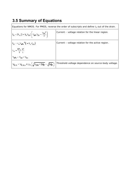
- Page 59 and 60: 4.7 Summary of Equations where wher
- Page 61 and 62: 5.1 DC (Bias) Circuit Dc circuits f
- Page 63 and 64: Thus, the negative sign in (5.1) is
- Page 65 and 66: and The "exact" equations of gm and
- Page 67 and 68: graph has plots of the output chara
- Page 69 and 70: 5.4 Current-Source Common-Source Am
- Page 71 and 72: The gain for this case is thus (neg
- Page 73 and 74: the drain current, ID, may be expre
- Page 75 and 76: V, δVtno = 0.1 V, and δkn = 100
- Page 77 and 78: 5.6 Summary of Equations av = -gmRD
- Page 79 and 80: Unit 6. Coupling and Bypass Capacit
- Page 81 and 82: 6.2 Current-Source Bias Amplifier:
- Page 83 and 84: 6.3 Precision Formulation of the Lo
- Page 85: Figure 6.4. (a) Equivalent circuit
- Page 88 and 89: 6.6 Exercises and Projects Project
- Page 90 and 91: 7.1 DC (Bias) Circuit The circuit d
- Page 92 and 93:
the "gain" (the transfer function i
- Page 94 and 95:
With the substitution of (4.11) in
- Page 96 and 97:
7.5 Exercises and Projects Project
- Page 98 and 99:
8.1 DC (Bias) Circuit The equation
- Page 100 and 101:
Using these definitions along with
- Page 102 and 103:
As always, the relation between the
- Page 104 and 105:
Equation 8.20 where the right-hand
- Page 106 and 107:
8.6 Common-Mode Voltage Gain The co
- Page 108 and 109:
This is the portion of current sour
- Page 110 and 111:
which gives Equation 8.38 Note that
- Page 112 and 113:
8.8 Body Effect and Voltage Gain In
- Page 114 and 115:
Note that in the absence of gds2, t
- Page 116 and 117:
8.10 Comparison of Numerical Gain R
- Page 118 and 119:
Rs = Ris2 || Rbias av2 = avsfavcg D
- Page 120 and 121:
Unit 9. MOSFET Current Sources With
- Page 122 and 123:
and W2 and W3 are the transistor ga
- Page 124 and 125:
transistor symbol represents the id
- Page 126 and 127:
9.3 Differential Amplifier Balancin
- Page 128 and 129:
9.4 Summary of Equations Reference
- Page 130 and 131:
10.1 DC (Bias) Circuit The bias cir
- Page 132 and 133:
Increasing gain is achieved with de
- Page 134 and 135:
10.4 Exercises and Projects Project
- Page 136 and 137:
11.1 Operational Amplifiers with Re
- Page 138 and 139:
Equation 11.4 AvNI is the limiting
- Page 140 and 141:
11.2 Output Resistance of the Resis
- Page 142 and 143:
11.4 DC Stabilization with the Feed
- Page 144 and 145:
11.5 Frequency Response of the Oper
- Page 146 and 147:
11.6 Summary of Equations T = avo/A
- Page 148 and 149:
Unit 12. Operational Amplifier Appl
- Page 150 and 151:
Equation 12.4 The 2 Vopeak is due t
- Page 152 and 153:
12.2 Operational Amplifier Oscillat
- Page 154 and 155:
Following the reasoning that led to
- Page 156 and 157:
12.3 Summary of Equations Opamp-int
- Page 158 and 159:
Unit 13. Cascaded Amplifier Stages
- Page 160 and 161:
13.2 Amplifier Gain of Differential
- Page 162 and 163:
Equation 13.5 For example, we set V
- Page 164 and 165:
13.4 Common-Source Stage as a Serie
- Page 166 and 167:
13.5 Shunt - Series Cascade Amplifi
- Page 168 and 169:
13.5.3 Signal Current Gain We first
- Page 170 and 171:
13.6 Summary of Equations , Gain of
- Page 172 and 173:
14.1 Current-Source Bias for the Di
- Page 174 and 175:
where Rbias is the bias resistor of
- Page 176 and 177:
Equation 14.8 The overall amplifier
- Page 178 and 179:
But Id1 = -Id4 and Id4 is mirrored
- Page 180 and 181:
where vD5 = vD2, as they are the sa
- Page 182 and 183:
Assume that W11 has been picked to
- Page 184 and 185:
The gain expression of the source f
- Page 186 and 187:
14.7 Output Resistance of the Feedb
- Page 188 and 189:
14.8 Output Circuit of the TS271 Op
- Page 190 and 191:
The output resistance of the circui
- Page 192 and 193:
Bias equation for differential ampl
- Page 195 and 196:
A.1 Basics of Sending and Receiving
- Page 197 and 198:
Front Panel Tools Palette Controls
- Page 199 and 200:
Initially, the Sequence Structure i
- Page 201 and 202:
Get the Wiring Tool (appears like a
- Page 203 and 204:
To install the Waveform graph, in t
- Page 205 and 206:
A.2 ADC and the Autoranging Voltmet
- Page 207 and 208:
A.3 LabVIEW Oscilloscope and Voltme
- Page 209 and 210:
A.4 Measuring the Discrete Characte
- Page 211 and 212:
A.5 Sending and Receiving Waveforms
- Page 213 and 214:
A.6 Summary of Programming Projects
- Page 215 and 216:
B.1 Fundamentals of Bipolar Junctio
- Page 217 and 218:
left (as in Fig. B.2). In practice,
- Page 219 and 220:
In electronic amplifiers, all three
- Page 221 and 222:
B.3 BJT Base, Emitter, and Collecto
- Page 223 and 224:
Note that the base current does not
- Page 225 and 226:
B.4 Diode-Connected Transistor Circ
- Page 227 and 228:
ISEprime vary, depending on the giv
- Page 229 and 230:
symmetrical in IC and IE and neglec
- Page 231 and 232:
where a new definition of a sort of
- Page 233 and 234:
Equation B.30 while for large VCE,
- Page 235 and 236:
A value for βR can be obtained, us
- Page 237 and 238:
B.9 Signal or Incremental Common-Em
- Page 239 and 240:
B.11 Exercises and Projects Project
- Page 241 and 242:
C.1 DC (Bias) Analysis The two comm
- Page 243 and 244:
C.2 Linear or Signal Model for the
- Page 245 and 246:
C.2.1 Determination of the Linear M
- Page 247 and 248:
C.3 Amplifier Voltage Gain Any tran
- Page 249 and 250:
Equation C.23 An additional approxi
- Page 251 and 252:
esult, for the positive and negativ
- Page 253 and 254:
C.6 Selection of Coupling Capacitor
- Page 255 and 256:
type of corner frequency, as it rep
- Page 257 and 258:
A signal impressed at the base of t
- Page 259 and 260:
The generalized gain expression, wh
- Page 261 and 262:
where Rop is the signal resistance
- Page 263 and 264:
C.8 Frequency Response of NPN - PNP
- Page 265 and 266:
Mathcad-generated plots of the magn
- Page 267 and 268:
C.9 Common-Emitter Stage with Emitt
- Page 269 and 270:
Equation C.74 The result shows that
- Page 271 and 272:
C.10 Summary of BJT Model Parameter
- Page 273 and 274:
Base current equation for commonemi
- Page 275 and 276:
Laboratory Project 1. Basic Circuit
- Page 277 and 278:
• Open a new VI to construct your
- Page 279 and 280:
an icon is displayed while the Wiri
- Page 281 and 282:
P1.2 Resistor Voltage Divider with
- Page 283 and 284:
P1.3 Resistor Voltage Divider with
- Page 285 and 286:
Procedure • Run the VI_03.vi for
- Page 287 and 288:
P1.5 Frequency Response of a Resist
- Page 289 and 290:
Laboratory Project 2. Basic NMOS Co
- Page 291 and 292:
Components Programming Exercise 2.1
- Page 293:
Procedure according to their functi
- Page 296 and 297:
Procedure • Run AmpP2.2.vi with V
- Page 298 and 299:
Press Ctrl and drag (with Arrow Too
- Page 300 and 301:
Laboratory Project 3. Characterizat
- Page 302 and 303:
P3.2 SPICE Equations SPICE Equation
- Page 304 and 305:
P3.4 Low-Voltage Linear Region of t
- Page 306 and 307:
P3.5 PMOS Parameters from the Trans
- Page 308 and 309:
P3.6 PMOS Lambda from the Transfer
- Page 310 and 311:
P3.7 PMOS Output Characteristic Com
- Page 312 and 313:
P3.8 PMOS Lambda LabVIEW Computatio
- Page 314 and 315:
P4.1 SPICE Parameters and Chip Diag
- Page 316 and 317:
P4.3 SPICE Equations SPICE Equation
- Page 318 and 319:
µA. Test run NMOSparsub.vi with VD
- Page 320 and 321:
Procedure • Set RS. Run NMOSparam
- Page 322 and 323:
P4.7 NMOS Gamma Components LabVIEW
- Page 324 and 325:
P4.8 NMOS Circuit with Body Effect
- Page 326 and 327:
Laboratory Project 5. PMOS Common-
- Page 328:
P5.2 PMOS Common-Source Amplifier D
- Page 331 and 332:
the Front Panel. Default and save.
- Page 333 and 334:
Procedure • Run Gain.vi to run Ga
- Page 335 and 336:
P6.1 PMOS Schematic and Pin Diagram
- Page 337:
P6.3 PMOS Current-Source Amplifier
- Page 340 and 341:
Procedure • The SubVI of Gain.vi,
- Page 342 and 343:
Laboratory Project 7. NMOS Common-
- Page 344:
P7.2 NMOS Common-Source Amplifier D
- Page 347 and 348:
Procedure (Obtain Parameters and Bi
- Page 349 and 350:
associated index. Then determine th
- Page 351 and 352:
XYtoDataFile2.vi. (Note that with t
- Page 353 and 354:
P8.1 SPICE Equations and Pin Diagra
- Page 356 and 357:
P8.3 Source-Follower Voltage Transf
- Page 358 and 359:
P8.4 Source-Follower Voltage Transf
- Page 360 and 361:
P9.1 SPICE Equations and Pin Diagra
- Page 362 and 363:
• After completing the circuit co
- Page 364 and 365:
P9.4 Amplifier Gain Measurement Pro
- Page 366 and 367:
P9.5 Transistor Parameters and DC I
- Page 368 and 369:
P9.6 Common-Mode Gain Measurement P
- Page 370 and 371:
P10.1 SPICE Equations and Pin Diagr
- Page 372 and 373:
P10.3 Evaluation of the Mirror-Curr
- Page 374:
P10.5 Measurement of the Amplifier
- Page 377 and 378:
P11.1 SPICE Equations SPICE Equatio
- Page 379 and 380:
Procedure • Do not initially turn
- Page 381 and 382:
Input Offset Voltage Vo = 1.4 V, Vi
- Page 383 and 384:
P11.5 Evaluation of the Gain and Si
- Page 385 and 386:
VOL Low-level output voltage (Vid =
- Page 387 and 388:
Large-signal voltage gain Vo = 1 to
- Page 389 and 390:
Gain - Bandwidth product (Av = 40 d
- Page 391 and 392:
P12.1 SPICE Equations SPICE Equatio
- Page 393 and 394:
Procedure • Connect the circuit,
- Page 395 and 396:
• Run OscOscill.vi to verify that
- Page 397 and 398:
PA.1 Sending and Receiving Voltages
- Page 400 and 401:
PA.3 Plotting Measured Samples •
- Page 402 and 403:
PA.4 Using the Autoranging Voltmete
- Page 404 and 405:
PA.6 Discrete Output Voltage from t
- Page 406 and 407:
PA.7 Discrete Input Voltage from th
- Page 408 and 409:
PA.8 Using the Simultaneous Sending
- Page 410 and 411:
PB.1 SPICE Parameters and Transisto
- Page 412 and 413:
PB.3 Diode-Connected Transistor Mea
- Page 414 and 415:
VBE on the high end, such that the
- Page 416 and 417:
PB.5 BJT Output Characteristic Meas
- Page 418 and 419:
PB.6 Simulation of the Output Chara
- Page 420 and 421:
PC.1 SPICE Equations and Pin Diagra
- Page 422 and 423:
IC_VCE_C.vi and set in RC and RB an
- Page 424 and 425:
Chan2_in for reading for reading th
- Page 426 and 427:
PC.5 Gain-Measurement Frequency Res
- Page 428 and 429:
Laboratory Project C2. NPN - PNP Co
- Page 430 and 431:
PC.7 Measurement of the PNP Paramet
- Page 432 and 433:
PC.8 DC Circuit Setup Components NP
- Page 434 and 435:
PC.9 Measurement of the Amplifier G