- Page 2 and 3: Day 1 Introduction of Mixed-Signal
- Page 4 and 5: SoC IP Based Design CORE Zone 4: Gl
- Page 7 and 8: Sensor Analog chip Sensor Integrati
- Page 9 and 10: Challenge of Integration • High d
- Page 11 and 12: Conventional Design Concept for Blo
- Page 13: Digital Model Abstraction Digital m
- Page 17 and 18: Analog Model Abstraction Circuit le
- Page 19 and 20: What Can Be Expected with Mixed-Sig
- Page 21 and 22: What is Required for Mixed-Signal S
- Page 23 and 24: To perform Multi-level Mixed-Signal
- Page 25 and 26: Lock-Step Fixed Time Roll-Back1 Rol
- Page 27: Integrated Single Kernel Mixed-Sign
- Page 30 and 31: Reference for Affirma Flow Use cdsd
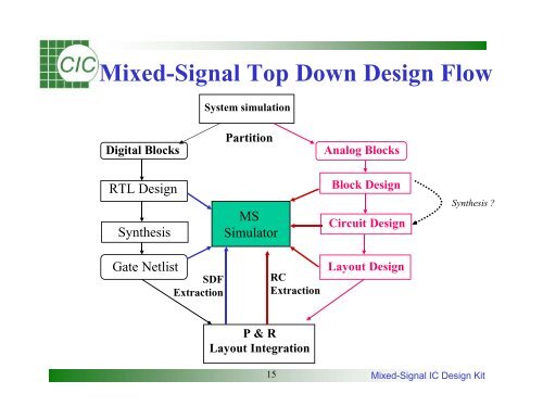
- Page 32 and 33: Mixed-Signal Top Down Design Flow S
- Page 34 and 35: The system is separated into blocks
- Page 36 and 37: Design Partitioning Scheme • The
- Page 38 and 39: Analog block Interface Element Sche
- Page 40 and 41: Using Analog Artist Environment for
- Page 42 and 43: Analog/Mixed Signal Description •
- Page 44 and 45: A module represents the fundamental
- Page 46 and 47: Verilog-A Modeling Approaches Struc
- Page 48 and 49: config Verilog-A Verilog-A Debugger
- Page 50 and 51: Component structure and behavioral
- Page 52 and 53: Saving HDL Design • For behaviora
- Page 54 and 55: Parameter Definition parameter defi
- Page 56 and 57: symbol rlc behavioral Verilog-A Mod
- Page 58 and 59: 58 Mixed-Signal IC Design Kit
- Page 60 and 61: Use “Save Generated Code” to st
- Page 62 and 63: The Analog Stimulus can be added ei
- Page 64 and 65:
symbol Instance 1 veriloga veriloga
- Page 66 and 67:
1. Use Template sample information
- Page 69 and 70:
Set Instance Binding With menu Hier
- Page 72 and 73:
Define Detailed Interface Elements
- Page 74:
Configuration of HE Display The con
- Page 77 and 78:
With Setup window to define simulat
- Page 79 and 80:
Interface Element Model Definition
- Page 81 and 82:
Level 2 Digital to Analog Interface
- Page 83 and 84:
MOS1_a2d Analog to Digital Interfac
- Page 85:
Device Model Specification The acti
- Page 88 and 89:
Define the analysis type through th
- Page 90 and 91:
Created Netlist(Analog) HNL : Hiera
- Page 92 and 93:
Simulation Options for Analog Simul
- Page 94 and 95:
Submit the Simulation Execute the s
- Page 96 and 97:
Result Browser After several simula
- Page 98 and 99:
Waveform Calculator If further calc
- Page 100 and 101:
For the HDL design, the Verilog-A i
- Page 102 and 103:
Layout Integration and Verification
- Page 104 and 105:
• LEF file • Verilog file • C
- Page 106 and 107:
LEF File of TSMC .35um 2P4M • Dig
- Page 108 and 109:
Cadence Abstract Generator Flow Ent
- Page 110 and 111:
Opening a Library • Included in t
- Page 112 and 113:
Distributing Cells • Central to t
- Page 114 and 115:
• Abstract: Generating Abstracts
- Page 116 and 117:
Exporting • If you are using Sili
- Page 118 and 119:
Prepare Data for SE : Verilog File
- Page 120:
• Since there might not be any Ve
- Page 123 and 124:
• Definition: Prepare Data for SE
- Page 125 and 126:
(HEADER… ) (GLOBAL … (Subset Ti
- Page 127 and 128:
Compiled TLF File • SE only reads
- Page 129 and 130:
Layout Integration • After prepar
- Page 131 and 132:
SE Startup • Before start SE, cre
- Page 133 and 134:
Import Timing Library • After APR
- Page 135 and 136:
Initiate Floorplan • Set the two
- Page 137 and 138:
Plan Power • Use Route Plan Powe
- Page 139 and 140:
Add IO Filler • Connect io pad po
- Page 141 and 142:
• Stripe Connect Rings - Connect
- Page 143 and 144:
Verification for Mixed-Signal Desig
- Page 145 and 146:
Read into DFII Library • After ex
- Page 147 and 148:
Export Layout • In Virtuoso, dele
- Page 149 and 150:
Calibre LVS Flow • Using “v2lvs
- Page 151 and 152:
Post-Layout Simulation for Mixed-Si
- Page 153 and 154:
Flows for Parasitic Simulation •
- Page 155 and 156:
Prepare layout Replace Layout View
- Page 157:
Reference • Mixed-Mode Simulation