PhD Thesis Arne Lüker final version V4 - Cranfield University
PhD Thesis Arne Lüker final version V4 - Cranfield University
PhD Thesis Arne Lüker final version V4 - Cranfield University

You also want an ePaper? Increase the reach of your titles
YUMPU automatically turns print PDFs into web optimized ePapers that Google loves.
Sol-Gel derived Ferroelectric Thin Films for Voltage Tunable Applications<br />
1 1 1<br />
tan δ device = = + , with Q<br />
Q Q Q<br />
device<br />
dielectric<br />
electrode<br />
electrode ω<br />
1<br />
= [Eq. 5.1]<br />
R C<br />
with Rs the series resistance of the electrodes. It should be clear that a low electrode<br />
resistivity means a high electrode quality factor and thus a low total device loss.<br />
Fan et al. [11, 12] has confirmed this concept as described in section 4.1. However, his<br />
realisation of a Cu bottom electrode for BST was relatively complicated due to the fact<br />
that different diffusion barrier layer were needed on either sides of the Cu electrode: a Ta<br />
diffusion barrier on top the Si substrate to inhibit Cu diffusion, and a TiAl layer as barrier<br />
against oxygen diffusion into the Cu layer to inhibit Cu oxidation during the deposition<br />
and annealing of the BST thin film.<br />
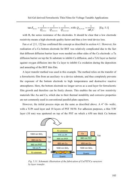
A layer transfer method was used in this example. The method relies on the transfer of<br />
a ferroelectric film from an auxiliary- to a device substrate, and thus completely prevents<br />
the exposure of the bottom electrode to high temperatures and destructive reactive<br />
atmospheres. Here, the bottom electrode no longer serves as a seed layer for ferroelectric<br />
film growth and therefore can be freely chosen. This enables the use of low resistivity<br />
materials like Au and Cu, which due to their thermal instability and corrosive properties<br />
are not commonly used in conventional parallel-plate capacitors.<br />
However, the initial process steps are the same as described above. A 4’’-Si- wafer,<br />
with a Ti/Pt seed layer and 10 layers of PST 50/50. For adhesion purposes, a thin TiW<br />
layer (10 nm) was sputtered on top of the PST on which a 650 nm thick Cu bottom<br />
1000 nm SiO2<br />
650 nm Cu<br />
660 nm PST<br />
100 nm Pt<br />
Si substrate<br />
TiW<br />
TiW<br />
Ti<br />
Si substrate<br />
100 nm Pt<br />
660 nm PST<br />
650 nm Cu<br />
1000 nm SiO2<br />
Quartz<br />
Cu<br />
S<br />
660 nm PST<br />
650 nm Cu<br />
1000 nm SiO2<br />
Quartz<br />
Fig. 5.11: Schematic illustration of the fabrication of Cu/PST/Cu varactors<br />
by layer transfer<br />
TiW<br />
103