PhD Thesis Arne Lüker final version V4 - Cranfield University
PhD Thesis Arne Lüker final version V4 - Cranfield University
PhD Thesis Arne Lüker final version V4 - Cranfield University

You also want an ePaper? Increase the reach of your titles
YUMPU automatically turns print PDFs into web optimized ePapers that Google loves.
136<br />
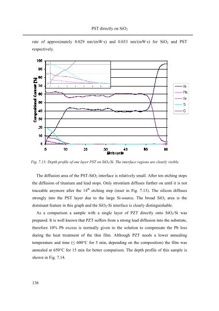
PST directly on SiO2<br />
rate of approximately 0.029 nm/(mW·s) and 0.033 nm/(mW·s) for SiO2 and PST<br />
respectively.<br />
Fig. 7.13: Depth profile of one layer PST on SiO2/Si. The interface regions are clearly visible.<br />
The diffusion area of the PST-SiO2 interface is relatively small. After ten etching steps<br />
the diffusion of titanium and lead stops. Only strontium diffuses further on until it is not<br />
traceable anymore after the 14 th etching step (inset in Fig. 7.13). The silicon diffuses<br />
strongly into the PST layer due to the large Si-source. The broad SiO2 area is the<br />
dominant feature in this graph and the SiO2-Si interface is clearly distinguishable.<br />
As a comparison a sample with a single layer of PZT directly onto SiO2/Si was<br />
prepared. It is well known that PZT suffers from a strong lead diffusion into the substrate,<br />
therefore 10% Pb excess is normally given to the solution to compensate the Pb loss<br />
during the heat treatment of the thin film. Although PZT needs a lower annealing<br />
temperature and time (≤ 600°C for 5 min, depending on the composition) the film was<br />
annealed at 650°C for 15 min for better comparison. The depth profile of this sample is<br />
shown in Fig. 7.14.