PhD Thesis Arne Lüker final version V4 - Cranfield University
PhD Thesis Arne Lüker final version V4 - Cranfield University
PhD Thesis Arne Lüker final version V4 - Cranfield University

You also want an ePaper? Increase the reach of your titles
YUMPU automatically turns print PDFs into web optimized ePapers that Google loves.
Sol-Gel derived Ferroelectric Thin Films for Voltage Tunable Applications<br />
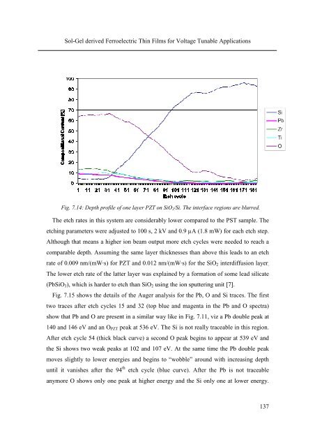
Fig. 7.14: Depth profile of one layer PZT on SiO2/Si. The interface regions are blurred.<br />
The etch rates in this system are considerably lower compared to the PST sample. The<br />
etching parameters were adjusted to 100 s, 2 kV and 0.9 µA (1.8 mW) for each etch step.<br />
Although that means a higher ion beam output more etch cycles were needed to reach a<br />
comparable depth. Assuming the same layer thicknesses than above this leads to an etch<br />
rate of 0.009 nm/(mW·s) for PZT and 0.012 nm/(mW·s) for the SiO2 interdiffusion layer.<br />
The lower etch rate of the latter layer was explained by a formation of some lead silicate<br />
(PbSiO3), which is harder to etch than SiO2 using the ion sputtering unit [7].<br />
Fig. 7.15 shows the details of the Auger analysis for the Pb, O and Si traces. The first<br />
two traces after etch cycles 15 and 32 (top blue and magenta in the Pb and O spectra)<br />
show that Pb and O are present in a similar way like in Fig. 7.11, viz a Pb double peak at<br />
140 and 146 eV and an OPZT peak at 536 eV. The Si is not really traceable in this region.<br />
After etch cycle 54 (thick black curve) a second O peak begins to appear at 539 eV and<br />
the Si shows two weak peaks at 102 and 107 eV. At the same time the Pb double peak<br />
moves slightly to lower energies and begins to “wobble” around with increasing depth<br />
until it vanishes after the 94 th etch cycle (blue curve). After the Pb is not traceable<br />
anymore O shows only one peak at higher energy and the Si only one at lower energy.<br />
137