PhD Thesis Arne Lüker final version V4 - Cranfield University
PhD Thesis Arne Lüker final version V4 - Cranfield University
PhD Thesis Arne Lüker final version V4 - Cranfield University

You also want an ePaper? Increase the reach of your titles
YUMPU automatically turns print PDFs into web optimized ePapers that Google loves.
Sol-Gel derived Ferroelectric Thin Films for Voltage Tunable Applications<br />
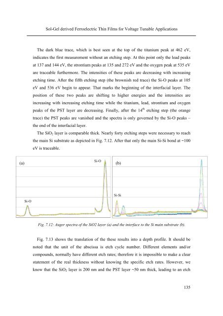
The dark blue trace, which is best seen at the top of the titanium peak at 462 eV,<br />
indicates the first measurement without an etching step. At this point only the lead peaks<br />
at 137 and 144 eV, the strontium peaks at 135 and 272 eV and the oxygen peak at 535 eV<br />
are traceable furthermore. The intensities of these peaks are decreasing with increasing<br />
etching time. After the fifth etching step (the brownish red trace) the Si-O peaks at 105<br />
eV and 536 eV begin to appear. That marks the beginning of the interfacial layer. The<br />
position of these two peaks are shifting to higher energies and the intensities are<br />
increasing with increasing etching time while the titanium, lead, strontium and oxygen<br />
peaks of the PST layer are decreasing. Finally, after the 14 th etching step (the orange<br />
trace) the PST peaks are vanished and the spectra is only governed by the Si-O peaks –<br />
the end of the interfacial layer.<br />
The SiO2 layer is comparable thick. Nearly forty etching steps were necessary to reach<br />
the main Si substrate as depicted in Fig. 7.12. After that only the main Si-Si bond at ~100<br />
eV is traceable.<br />
Si-O<br />
(a) (b)<br />
Si-O<br />
Si-Si<br />
Fig. 7.12: Auger spectra of the SiO2 layer (a) and the interface to the Si main substrate (b).<br />
Fig. 7.13 shows the translation of the these results into a depth profile. It should be<br />
noted that the unit of the abscissa is etch cycle number. Different elements and/or<br />
compounds, normally have different etch rates; therefore it is impossible to make a clear<br />
statement of the real thickness without knowing the specific etch rates. However, we<br />
know that the SiO2 layer is 200 nm and the PST layer ~50 nm thick, leading to an etch<br />
135