PhD Thesis Arne Lüker final version V4 - Cranfield University
PhD Thesis Arne Lüker final version V4 - Cranfield University
PhD Thesis Arne Lüker final version V4 - Cranfield University

You also want an ePaper? Increase the reach of your titles
YUMPU automatically turns print PDFs into web optimized ePapers that Google loves.
144<br />
PST as a buffer layer for PZT on SiO2<br />
sequentially may introduce damage to the device layers and degrade the properties of the<br />
functional materials. However there is a possibility in the modified process design that<br />
PZT may suffer from post-annealing issues such as PZT bubbling and microcracks during<br />
PZT crystallisation on non-uniform patterned Pt/Ti/SiO2/Si substrates. A crack-free PST<br />
layer as a diffusion buffer could prevent PZT bubbling during PZT crystallisation on a<br />
patterned Si substrate and is expected to be beneficial to wafer-scale integration of the<br />
PZT microdevices. In addition, high quality PST films can be deposited cheaper with<br />
easy composition control using sol-gel technique, similar to PZT films deposition, thus<br />
reducing the process complexity, undesired damage to PZT device layers and overall<br />
process time.<br />
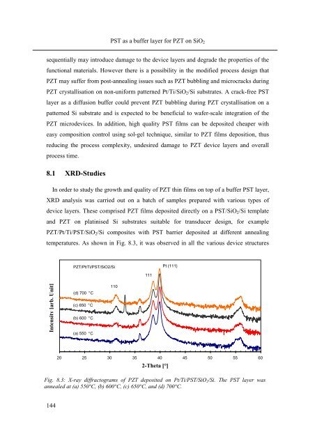
8.1 XRD-Studies<br />
In order to study the growth and quality of PZT thin films on top of a buffer PST layer,<br />
XRD analysis was carried out on a batch of samples prepared with various types of<br />
device layers. These comprised PZT films deposited directly on a PST/SiO2/Si template<br />
and PZT on platinised Si substrates suitable for transducer design, for example<br />
PZT/Pt/Ti/PST/SiO2/Si composites with PST barrier deposited at different annealing<br />
temperatures. As shown in Fig. 8.3, it was observed in all the various device structures<br />
Intensity [arb. Unit]<br />
PZT/Pt/Ti/PST/SiO2/Si<br />
(d) 700 °C<br />
(c) 650 °C<br />
(b) 600 °C<br />
(a) 550 °C<br />
110<br />
111<br />
Pt (111)<br />
20 25 30 35 40 45 50 55 60<br />
2-Theta [°]<br />
Fig. 8.3: X-ray diffractograms of PZT deposited on Pt/Ti/PST/SiO2/Si. The PST layer was<br />
annealed at (a) 550°C, (b) 600°C, (c) 650°C, and (d) 700°C.