PhD Thesis Arne Lüker final version V4 - Cranfield University
PhD Thesis Arne Lüker final version V4 - Cranfield University
PhD Thesis Arne Lüker final version V4 - Cranfield University

Create successful ePaper yourself
Turn your PDF publications into a flip-book with our unique Google optimized e-Paper software.
Sol-Gel derived Ferroelectric Thin Films for Voltage Tunable Applications<br />
PST directly on SiO2<br />
Ferroelectric thin films like PZT and BST often need a metallic like layer on top of the<br />
substrate to promote a crack-free and highly orientated growth. The most common<br />
metallic layer is Pt due to its high chemical resistance, relative good lattice match to the<br />
ferroelectric film, and its stability to the high temperatures required for the growth of<br />
ferroelectric thin films. Pt is a precious material and therefore a not insignificant part of<br />
the cumulative overall costs of ferroelectric devices and applications. Moreover,<br />
sometimes it is beneficial from the technological site of view to have the ability to work<br />
with a patterned bottom electrode rather than a continuous one.<br />
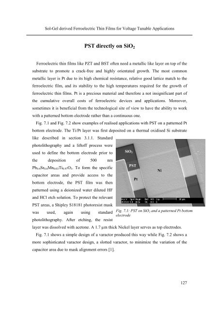
Fig. 7.1 and Fig. 7.2 show examples of realised applications with PST on a patterned Pt<br />
bottom electrode. The Ti/Pt layer was first deposited on a thermal oxidised Si substrate<br />
like described in section 3.1.1. Standard<br />
photolithography and a liftoff process were<br />
used to define the bottom electrode prior to<br />
the deposition of 500 nm<br />
Pb0.4Sr0.6Mn0.03Ti0.97O3. To form the specific<br />
capacitor areas and provide access to the<br />
bottom electrode, the PST film was then<br />
patterned using a deionized water diluted HF<br />
and HCl etch solution. To protect the relevant<br />
PST areas, a Shipley S18181 photoresist mask<br />
was used, again using standard<br />
photolithography. After etching, the resist<br />
layer was dissolved with acetone. A 1.7 µm thick Nickel layer serves as top electrodes.<br />
Fig. 7.1 shows a simple design of a varactor produced this way while Fig. 7.2 shows a<br />
more sophisticated varactor design, a slotted varactor, to minimize the variation of the<br />
capacitor area due to mask alignment errors [1].<br />
SiO2<br />
PST<br />
Pt<br />
Ni<br />
Fig. 7.1: PST on SiO2 and a patterned Pt bottom<br />
electrode<br />
127