PhD Thesis Arne Lüker final version V4 - Cranfield University
PhD Thesis Arne Lüker final version V4 - Cranfield University
PhD Thesis Arne Lüker final version V4 - Cranfield University

You also want an ePaper? Increase the reach of your titles
YUMPU automatically turns print PDFs into web optimized ePapers that Google loves.
Sol-Gel derived Ferroelectric Thin Films for Voltage Tunable Applications<br />
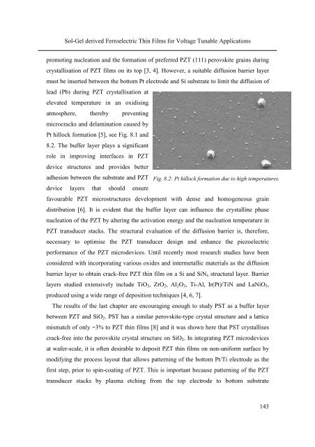
promoting nucleation and the formation of preferred PZT (111) perovskite grains during<br />
crystallisation of PZT films on its top [3, 4]. However, a suitable diffusion barrier layer<br />
must be inserted between the bottom Pt electrode and Si substrate to limit the diffusion of<br />
lead (Pb) during PZT crystallisation at<br />
elevated temperature in an oxidising<br />
atmosphere, thereby preventing<br />
microcracks and delamination caused by<br />
Pt hillock formation [5], see Fig. 8.1 and<br />
8.2. The buffer layer plays a significant<br />
role in improving interfaces in PZT<br />
device structures and provides better<br />
adhesion between the substrate and PZT<br />
device layers that should ensure<br />
favourable PZT microstructures development with dense and homogeneous grain<br />
distribution [6]. It is evident that the buffer layer can influence the crystalline phase<br />
nucleation of the PZT by altering the activation energy and the nucleation temperature in<br />
PZT transducer stacks. The structural evaluation of the diffusion barrier is, therefore,<br />
necessary to optimise the PZT transducer design and enhance the piezoelectric<br />
performance of the PZT microdevices. Until recently most research studies have been<br />
considered with incorporating various oxides and intermetallic materials as the diffusion<br />
barrier layer to obtain crack-free PZT thin film on a Si and SiNx structural layer. Barrier<br />
layers studied extensively include TiO2, ZrO2, Al2O3, Ti-Al, Ir(Pt)/TiN and LaNiO3,<br />
produced using a wide range of deposition techniques [4, 6, 7].<br />
Fig. 8.2: Pt hillock formation due to high temperatures.<br />
The results of the last chapter are encouraging enough to study PST as a buffer layer<br />
between PZT and SiO2. PST has a similar perovskite-type crystal structure and a lattice<br />
mismatch of only ~3% to PZT thin films [8] and it was shown here that PST crystallises<br />
crack-free into the perovskite crystal structure on SiO2. In integrating PZT microdevices<br />
at wafer-scale, it is often desirable to deposit PZT thin films on non-uniform surface by<br />
modifying the process layout that allows patterning of the bottom Pt/Ti electrode as the<br />
first step, prior to spin-coating of PZT. This is important because patterning of the PZT<br />
transducer stacks by plasma etching from the top electrode to bottom substrate<br />
143