PhD Thesis Arne Lüker final version V4 - Cranfield University
PhD Thesis Arne Lüker final version V4 - Cranfield University
PhD Thesis Arne Lüker final version V4 - Cranfield University

You also want an ePaper? Increase the reach of your titles
YUMPU automatically turns print PDFs into web optimized ePapers that Google loves.
Sol-Gel derived Ferroelectric Thin Films for Voltage Tunable Applications<br />
the other hand, contain some misoriented grains with (111) and (100) out-of-plane texture<br />
and electron diffraction patterns (not shown) indicate the presence of twins, defects that<br />
are quite common in Cu. No clear epitaxial relationship between the PST film and the Cu<br />
electrodes does exist.<br />
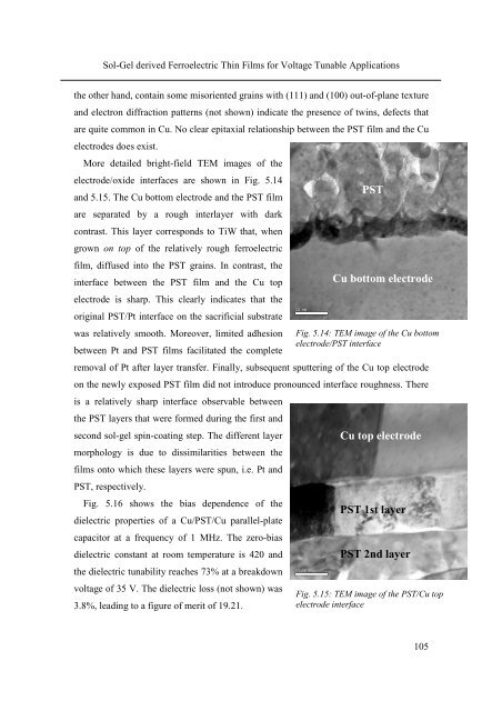
More detailed bright-field TEM images of the<br />
electrode/oxide interfaces are shown in Fig. 5.14<br />
and 5.15. The Cu bottom electrode and the PST film<br />
are separated by a rough interlayer with dark<br />
contrast. This layer corresponds to TiW that, when<br />
grown on top of the relatively rough ferroelectric<br />
film, diffused into the PST grains. In contrast, the<br />
interface between the PST film and the Cu top<br />
electrode is sharp. This clearly indicates that the<br />
original PST/Pt interface on the sacrificial substrate<br />
was relatively smooth. Moreover, limited adhesion<br />
between Pt and PST films facilitated the complete<br />
removal of Pt after layer transfer. Finally, subsequent sputtering of the Cu top electrode<br />
on the newly exposed PST film did not introduce pronounced interface roughness. There<br />
is a relatively sharp interface observable between<br />
the PST layers that were formed during the first and<br />
second sol-gel spin-coating step. The different layer<br />
morphology is due to dissimilarities between the<br />
films onto which these layers were spun, i.e. Pt and<br />
PST, respectively.<br />
Fig. 5.16 shows the bias dependence of the<br />
dielectric properties of a Cu/PST/Cu parallel-plate<br />
capacitor at a frequency of 1 MHz. The zero-bias<br />
dielectric constant at room temperature is 420 and<br />
the dielectric tunability reaches 73% at a breakdown<br />
voltage of 35 V. The dielectric loss (not shown) was<br />
3.8%, leading to a figure of merit of 19.21.<br />
PST<br />
Cu bottom electrode<br />
Fig. 5.14: TEM image of the Cu bottom<br />
electrode/PST interface<br />
Cu top electrode<br />
PST 1st layer<br />
PST 2nd layer<br />
Fig. 5.15: TEM image of the PST/Cu top<br />
electrode interface<br />
105