- Page 1 and 2: R /(mol m -2 s -1 ) 0.06 0.05 0.04
- Page 3 and 4: ANA-MARIA CORMOS, JOZSEF GASPAR, AN
- Page 5 and 6: Studia Universitatis Babes-Bolyai C
- Page 7 and 8: 6 PROFESSOR IOAN BÂLDEA AT HIS 70
- Page 9 and 10: MARCELA ACHIM, DANA MUNTEAN, LAURIA
- Page 11 and 12: MARCELA ACHIM, DANA MUNTEAN, LAURIA
- Page 13 and 14: MARCELA ACHIM, DANA MUNTEAN, LAURIA
- Page 15 and 16: STUDIA UNIVERSITATIS BABEŞ-BOLYAI,
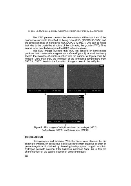
- Page 17 and 18: STUDIES ON WO3 THIN FILMS PREPARED
- Page 19: STUDIES ON WO3 THIN FILMS PREPARED
- Page 23 and 24: STUDIA UNIVERSITATIS BABEŞ-BOLYAI,
- Page 25 and 26: PREPARATION AND CHARACTERIZATION OF
- Page 27 and 28: PREPARATION AND CHARACTERIZATION OF
- Page 29 and 30: PREPARATION AND CHARACTERIZATION OF
- Page 31 and 32: 32 C. CĂŢĂNAŞ, M. MOGOŞ, D. HO
- Page 33 and 34: 34 C. CĂŢĂNAŞ, M. MOGOŞ, D. HO
- Page 35 and 36: C. CĂŢĂNAŞ, M. MOGOŞ, D. HORVA
- Page 37 and 38: 38 ANA-MARIA CORMOS, JOZSEF GASPAR,
- Page 39 and 40: ANA-MARIA CORMOS, JOZSEF GASPAR, AN
- Page 41 and 42: 42 ANA-MARIA CORMOS, JOZSEF GASPAR,
- Page 43 and 44: 44 ANA-MARIA CORMOS, JOZSEF GASPAR,
- Page 45 and 46: 46 ANA-MARIA CORMOS, JOZSEF GASPAR,
- Page 47 and 48: 48 ANA-MARIA CORMOS, JOZSEF GASPAR,
- Page 49 and 50: 50 EUGEN DARVASI, LADISLAU KÉKEDY-
- Page 51 and 52: 52 EUGEN DARVASI, LADISLAU KÉKEDY-
- Page 53 and 54: 54 EUGEN DARVASI, LADISLAU KÉKEDY-
- Page 55 and 56: 56 EUGEN DARVASI, LADISLAU KÉKEDY-
- Page 57 and 58: 58 EUGEN DARVASI, LADISLAU KÉKEDY-
- Page 59 and 60: STUDIA UNIVERSITATIS BABEŞ-BOLYAI,
- Page 61 and 62: MATHEMATICAL MODELING FOR THE CRYST
- Page 63 and 64: MATHEMATICAL MODELING FOR THE CRYST
- Page 65 and 66: MATHEMATICAL MODELING FOR THE CRYST
- Page 67 and 68: MATHEMATICAL MODELING FOR THE CRYST
- Page 69 and 70: STUDIA UNIVERSITATIS BABEŞ-BOLYAI,
- Page 71 and 72:
STUDY OF THE CHROMATOGRAPHIC RETENT
- Page 73 and 74:
STUDY OF THE CHROMATOGRAPHIC RETENT
- Page 75 and 76:
STUDY OF THE CHROMATOGRAPHIC RETENT
- Page 77 and 78:
STUDY OF THE CHROMATOGRAPHIC RETENT
- Page 79 and 80:
STUDIA UNIVERSITATIS BABEŞ-BOLYAI,
- Page 81 and 82:
LOWER RIM SILYL SUBSTITUTED CALIX[8
- Page 83 and 84:
LOWER RIM SILYL SUBSTITUTED CALIX[8
- Page 85 and 86:
LOWER RIM SILYL SUBSTITUTED CALIX[8
- Page 87 and 88:
STUDIA UNIVERSITATIS BABEŞ-BOLYAI,
- Page 89 and 90:
THE INTERACTION OF SILVER NANOPARTI
- Page 91 and 92:
THE INTERACTION OF SILVER NANOPARTI
- Page 93 and 94:
THE INTERACTION OF SILVER NANOPARTI
- Page 95 and 96:
STUDIA UNIVERSITATIS BABEŞ-BOLYAI,
- Page 97 and 98:
OPTIMISATION OF COPPER REMOVAL FROM
- Page 99 and 100:
OPTIMISATION OF COPPER REMOVAL FROM
- Page 101 and 102:
OPTIMISATION OF COPPER REMOVAL FROM
- Page 103 and 104:
OPTIMISATION OF COPPER REMOVAL FROM
- Page 105 and 106:
MELINDA-HAYDEE KOVACS, DUMITRU RIST
- Page 107 and 108:
MELINDA-HAYDEE KOVACS, DUMITRU RIST
- Page 109 and 110:
MELINDA-HAYDEE KOVACS, DUMITRU RIST
- Page 111 and 112:
MELINDA-HAYDEE KOVACS, DUMITRU RIST
- Page 113 and 114:
STUDIA UNIVERSITATIS BABEŞ-BOLYAI,
- Page 115 and 116:
IRON DOPED CARBON AEROGEL AS CATALY
- Page 117 and 118:
IRON DOPED CARBON AEROGEL AS CATALY
- Page 119 and 120:
IRON DOPED CARBON AEROGEL AS CATALY
- Page 121 and 122:
IRON DOPED CARBON AEROGEL AS CATALY
- Page 123 and 124:
128 ANDRADA MĂICĂNEANU, HOREA BED
- Page 125 and 126:
130 ANDRADA MĂICĂNEANU, HOREA BED
- Page 127 and 128:
132 ANDRADA MĂICĂNEANU, HOREA BED
- Page 129 and 130:
134 ANDRADA MĂICĂNEANU, HOREA BED
- Page 131 and 132:
ANDRADA MĂICĂNEANU, HOREA BEDELEA
- Page 133 and 134:
138 ANDRADA MĂICĂNEANU, HOREA BED
- Page 135 and 136:
140 ANDRADA MĂICĂNEANU, HOREA BED
- Page 137 and 138:
CRISTINA MIHALI, GABRIELA OPREA, EL
- Page 139 and 140:
144 CRISTINA MIHALI, GABRIELA OPREA
- Page 141 and 142:
146 Interfering ion, J - I - DBS -
- Page 143 and 144:
CONCLUSIONS 148 CRISTINA MIHALI, GA
- Page 145 and 146:
150 CRISTINA MIHALI, GABRIELA OPREA
- Page 147 and 148:
152 D. MIHU, L. VLASE, S. IMRE, C.
- Page 149 and 150:
154 Intens. x105 1.5 1.0 0.5 0.0 x1
- Page 151 and 152:
D. MIHU, L. VLASE, S. IMRE, C. M. M
- Page 153 and 154:
158 D. MIHU, L. VLASE, S. IMRE, C.
- Page 155 and 156:
160 D. MIHU, L. VLASE, S. IMRE, C.
- Page 157 and 158:
162 A. PETER, M. BAIA, F. TODERAS,
- Page 159 and 160:
164 (a) V relative [%] (c) V relati
- Page 161 and 162:
A. PETER, M. BAIA, F. TODERAS, M. L
- Page 163 and 164:
168 A. PETER, M. BAIA, F. TODERAS,
- Page 165 and 166:
170 A. PETER, M. BAIA, F. TODERAS,
- Page 167 and 168:
STUDIA UNIVERSITATIS BABEŞ-BOLYAI,
- Page 169 and 170:
BIOSORPTION OF PHENOL FROM AQUEOUS
- Page 171 and 172:
BIOSORPTION OF PHENOL FROM AQUEOUS
- Page 173 and 174:
BIOSORPTION OF PHENOL FROM AQUEOUS
- Page 175 and 176:
BIOSORPTION OF PHENOL FROM AQUEOUS
- Page 177 and 178:
BIOSORPTION OF PHENOL FROM AQUEOUS
- Page 179 and 180:
186 ANDREI ROTARU, MIHAI GOŞA, EUG
- Page 181 and 182:
188 ANDREI ROTARU, MIHAI GOŞA, EUG
- Page 183 and 184:
ANDREI ROTARU, MIHAI GOŞA, EUGEN S
- Page 185 and 186:
192 ANDREI ROTARU, MIHAI GOŞA, EUG
- Page 187 and 188:
194 OCTAVIAN STAICU, VALENTIN MUNTE
- Page 189 and 190:
ln(τ i / s) OCTAVIAN STAICU, VALEN
- Page 191 and 192:
198 OCTAVIAN STAICU, VALENTIN MUNTE
- Page 193 and 194:
200 OCTAVIAN STAICU, VALENTIN MUNTE
- Page 195 and 196:
202 OCTAVIAN STAICU, VALENTIN MUNTE
- Page 197 and 198:
204 MARIA ŞTEFAN, IOAN BÂLDEA, RO
- Page 199 and 200:
206 MARIA ŞTEFAN, IOAN BÂLDEA, RO
- Page 201 and 202:
208 MARIA ŞTEFAN, IOAN BÂLDEA, RO
- Page 203 and 204:
EXPERIMENTAL SECTION 210 MARIA ŞTE
- Page 205 and 206:
STUDIA UNIVERSITATIS BABEŞ-BOLYAI,
- Page 207 and 208:
EQUILIBRIUM STUDY ON ADSORPTION PRO
- Page 209 and 210:
EQUILIBRIUM STUDY ON ADSORPTION PRO
- Page 211 and 212:
EQUILIBRIUM STUDY ON ADSORPTION PRO
- Page 213 and 214:
EQUILIBRIUM STUDY ON ADSORPTION PRO
- Page 215 and 216:
STUDIA UNIVERSITATIS BABEŞ-BOLYAI,
- Page 217 and 218:
STRATEGIES OF HEAVY METAL UPTAKE BY
- Page 219 and 220:
STRATEGIES OF HEAVY METAL UPTAKE BY
- Page 221 and 222:
STRATEGIES OF HEAVY METAL UPTAKE BY
- Page 223 and 224:
STRATEGIES OF HEAVY METAL UPTAKE BY
- Page 225 and 226:
STRATEGIES OF HEAVY METAL UPTAKE BY
- Page 227 and 228:
STUDIA UNIVERSITATIS BABEŞ-BOLYAI,
- Page 229 and 230:
CORROSION INHIBITION OF BRONZE BY A
- Page 231 and 232:
CORROSION INHIBITION OF BRONZE BY A
- Page 233 and 234:
CORROSION INHIBITION OF BRONZE BY A
- Page 235 and 236:
CORROSION INHIBITION OF BRONZE BY A
- Page 237 and 238:
CORROSION INHIBITION OF BRONZE BY A
- Page 239 and 240:
STUDIA UNIVERSITATIS BABEŞ-BOLYAI,
- Page 241 and 242:
E / mV vs. SCE POTASSIUM-SELECTIVE
- Page 243 and 244:
POTASSIUM-SELECTIVE ELECTRODE BASED
- Page 245 and 246:
POTASSIUM-SELECTIVE ELECTRODE BASED
- Page 247 and 248:
256 CODRUTA VARODI, DELIA GLIGOR, L
- Page 249 and 250:
CODRUTA VARODI, DELIA GLIGOR, LEVEN
- Page 251 and 252:
260 CODRUTA VARODI, DELIA GLIGOR, L
- Page 253 and 254:
262 CODRUTA VARODI, DELIA GLIGOR, L
- Page 255 and 256:
STUDIA UNIVERSITATIS BABEŞ-BOLYAI,
- Page 257 and 258:
PHARMACOKINETIC INTERACTION BETWEEN
- Page 259 and 260:
PHARMACOKINETIC INTERACTION BETWEEN
- Page 261:
PHARMACOKINETIC INTERACTION BETWEEN